Quantcast
Channel: stm32 – Andys Workshop
Viewing all 25 articles
Browse latest View live

stm32plus 2.1.0

$
0
0

The latest release is now 3.0.0. Be sure to check out the announcement here.

Due to the use of c++0x features the minimum compiler requirement is now version 4.7.0 of gcc


stm32plus version 2.1.0 has now been released and is available from my downloads page. This article will present a brief overview of the following new features.

  • LGDP453x TFT driver
  • SSD1289 TFT driver
  • SSD1963 TFT driver
  • ST7783 TFT driver
  • AT24C32/64 serial EEPROM support

As mentioned in the banner at the top of this page you will need to ensure that you are using at least version 4.7.0 of gcc. I’m currently working on a driver for one of the big on-chip peripherals and it just couldn’t be done cleanly without real variadic templates so I took the opportunity to migrate all the template ‘feature’ mix-in classes to variadics. I also replaced lots of subclass types that were there as a workaround for the lack of template typedefs with much cleaner template aliases.

I use the free ‘arm-2012.09′ arm-none-eabi gcc release supplied by CodeSourcery (aka. Mentor Graphics) on Windows 7 x64 and Ubuntu Linux and I recommend that you do too. Other gcc toolchains may also work but are not tested. non-gcc compilers will certainly not work.

The installation and usage instructions have not changed since version 2.0.0. Documentation can be found in this previous article.

LGDP453x TFT driver

The LGDP4531/2 is a 320×240 (QVGA) TFT panel from LG. The stm32plus driver for this panel was contributed by Andy Franz and gratefully accepted by myself into this release.

64K and 262K colour modes are supported in landscape and portrait orientations. A full list of driver declarations are:

LGDP453x_Portrait_64K
LGDP453x_Landscape_64K
LGDP453x_Portrait_262K
LGDP453x_Landscape_262K

Andy created a corresponding example demo that you can find in the ‘examples/lgdp453x’ directory.

SSD1289 TFT driver

Experimental support is now provided for the Solomon Systech 1289 QVGA TFT driver with 64K and 262K colours and in landscape and portrait mode. The driver names are:

SSD1289_Portrait_64K
SSD1289_Landscape_64K
SSD1289_Portrait_262K
SSD1289_Landscape_262K

An example demo program is supplied in the ‘examples/ssd1289′ directory.

I have labelled this driver as experimental because I have not been able to verify that it works with the cheap ebay SSD1289 panel that I have because my cheap panel appears to be hardwired into an interlaced mode.

That is, if you set a display window to cover the whole screen and then fill it with pixels then the pixels will fill the rows in this order: 1,0,3,2,5,4… This makes it impossible to support with my graphics driver.

The offending driver input line is ‘GD’ and of course it’s the only one you can’t set in software using the ‘driver output control (r01h)’ register. Hopefully one of you will have a panel with ‘GD’ set to the non-interlaced mode!

SSD1963 TFT driver

The SSD1963 is another one from Solomon Systech. It’s slightly unusual in that it’s not hard-wired to any particular resolution. Instead it allows you to program it to support any resolution up to 800×480 as long as you know the timings for the panel that you’re going to use.

The stm32plus driver for the SSD1963 calls upon small ‘traits’ classes to supply the timing and size information for the panel being controlled. My test panel is a 4.3″ 480×272 device obtained on ebay and I have supplied traits classes for it. The driver names are:

SSD1963_480x272_Portrait_262K
SSD1963_480x272_Landscape_262K
SSD1963_480x272_Portrait_16M
SSD1963_480x272_Landscape_16M

I’ve put together a short video of this panel in action connected to the STM32F103.

ST7783 TFT driver

I’ve got a cool new docking expansion board for my STM32F4DISCOVERY that adds some common peripherals to the system including an ethernet PHY, an RS232 socket, an SD cage and of course a QVGA LCD with a touch panel.

The driver IC for this panel is the ST7783 and I am pleased to announce support for it with 64K and 262K colours in portrait and landscape modes. The driver names are:

ST7783_Portrait_64K
ST7783_Landscape_64K
ST7783_Portrait_262K
ST7783_Landscape_262K

I also put together a short video that shows it in action. The F4 drives this panel very quickly indeed.

AT24C32/64 serial EEPROM support

Unlike some other devices such as the 8-bit AVRs the STM32 doesn’t have any EEPROM memory included on-chip although it is possible to emulate it to some extent by reading and writing the internal flash memory at runtime.

If you need real EEPROM support then you have to purchase and wire up an external IC.

The Atmel AT24C32 and AT24C64 are 32/64Kbit serial EEPROM devices that are controllable via an I2C bus. The STM32 I2C on-chip peripheral is ideally suited to communicating with these memories.

stm32plus provides two drivers named ‘AT24C32′ and ‘AT24C64′ to manage communication with these devices. Both drivers inherit from InputStream and OutputStream so you can use all the methods that the stream interfaces provide.

The driver class is templated with the I2C interface that you are going to use to communicate with it. An example declaration might be:

#include "config/stm32plus.h"
#include "config/i2c.h"
#include "config/eeprom.h"

typedef AT24C32<
  I2C2_Default<I2CTwoByteMasterPollingFeature>
> MyEeprom;

I2C::Parameters params;
MyEeprom eeprom(params);

A full example is included in the ‘examples/i2c_at24c32′ directory.

Changelog

Here’s the changelog for version 2.1.0 in full.

Added “TypeB” Nokia N95 8Gb driver (LDS285 controller). stm32plus now supports both types of this cellphone display that I’ve found so far.

Accepted LGDP453x TFT driver and demo contributed by Andy Franz. Thanks Andy!

Added drivers for SSD1289, SSD1963 and ST7783 LCD interfaces. Demos are included.

Change compile flags to C++0x with GNU extensions. This will facilitate a migration to variadic templates for the feature classes. The motivation for the migration is cleaner and smaller code generation.

Ported all peripheral classes that allowed template features to variadic templates.

Ported all LCD interface declarations from subclasses to template typedef aliases. Removed the colour depth suffix from graphic terminal class names, i.e. remove _64K, _262K suffixes. This is because there’s no difference between the colour depths making the suffix irrelevant.

Replaced SmartArray.h with scoped_array.h and scoped_ptr.h lifted from the open source Chromium project with appropriate credits.

Added reset() method to MillisecondTimer to bring the clock back down to zero.

Fixed STL slist for modern, stricter compilers.

Increased reliability of ADS7843 touch screen by preventing the pen interrupt from occurring while sampling is taking place.

Replaced the 3 GraphicTerminal* classes with a single GraphicTerminal template. The terminal declarations for each LCD interface have been updated accordingly. Graphics terminal declarations have now lost the colour depth suffix. So for example:

ILI9325_Terminal_Portrait_262K<LcdAccess> 

would now be:

  
ILI9325_Terminal_Portrait<LcdAccess>

Also, the terminal class constructor is now a reference and not a pointer.

Implemented AT24C32/64 serial EEPROM classes with I2C interface. An example program is provided. Include “config/eeprom.h” to get access to the class.

Created StreamBase base class for InputStream and OutputStream and lifted up the error codes into the base as well as the common close() interface method.


Update: bug notification

A bug has come to light that affects optimised builds. It’s too small for me to do a full release so I’ll explain here what you need to do to fix it.

The problem is that the counter used by the MillisecondTimer class should be declared volatile. You can fix it like this:

In stm32plus/include/timing/MillisecondTimer.h change the counter declaration to include ‘volatile’:

public:
  volatile static uint32_t _counter;

Also change it in the source file: stm32plus/src/timing/MillisecondTimer.cpp:

volatile uint32_t MillisecondTimer::_counter;

stm32plus::net, a C++ TCP/IP stack for the STM32

$
0
0

Welcome to a landmark release, version 3.0.0, of my stm32plus C++ library for the STM32F1 and STM32F4 series of microcontrollers.

This release introduces support for the ethernet MAC peripheral in the form of an object-oriented TCP/IP stack as well as support for the STM32F107 connectivity line of MCUs. Furthermore, all the source code is now available on github.com to enable easy browsing and collaborative development.

Read on for all the details.

stm32plus::net

It’s been some time now since I published the designs for my ethernet PHY for the STM32F107 based on the Micrel KSZ8051MLL.

I was naturally very pleased with the success of that design and at the same time frustrated that the only usable TCP/IP stack was LwIP. Now there’s nothing functionally wrong with LwIP, it does exactly what it sets out to do and works on a wide range of processors. My problems were that it’s just a bad fit for a C++ design, doesn’t gel well with modern programming techniques, and as a general solution it can never take full advantage of everything the STM32 MAC has to offer.

So I decided to dig out my nineteen year old hardback copy of TCP/IP illustrated and put my twenty years of commercial experience of programming against the TCP/IP protocols to use and write a completely new TCP/IP stack consisting of all original code and designed to be object-oriented, very fast and very efficient.

Several months-worth of weekend and evening hacking later and it’s ready. Here’s a non-exhaustive list of some of features.

  • ARP, IPv4, UDP, TCP, ICMP, DHCP, DNS, LLIP support.
  • KSZ8051MLL and DP83848C PHY support included in MII/RMII mode.
  • IP large packet fragmentation/reassembly support.
  • IP/TCP/UDP hardware checksum offload support.
  • Hardware MAC address filtering.
  • FTP and HTTP application layer examples included.

The design

A TCP/IP stack is a many-layered affair. Each layer builds on the capabilities of the one below it in order to present new functionality.

The picture shows the network stack as implemented by stm32plus. I say, as implemented by… because purists may notice that I’ve included ICMP in the transport layer and not the network layer. That’s because it requires the services of the network layer, specifically IP, to work so I’ve lifted it up into the transport layer. Really it straddles both transport and network layers.

Declarative implementation

A design goal was to emulate the operation of the layers as closely as possible and to allow the user to pick and choose the protocols required at compile-time. If there are any incompatibilities or missing components then the program should fail to compile.

I decided to use the C++0x variadic template feature to model the stack. Each layer has its own variadic template that you can configure with the components for that layer and have it link automatically to the layers below.

For example, the Transport layer template looks like this:

template<class TNetworkLayer,template<class> class... Features>
class TransportLayer : public virtual TNetworkLayer,
                       public Features<TNetworkLayer>... {

Don’t worry if the template syntax makes your head spin, that’s a normal reaction! What’s achieved here is that we pull in all the transport layer components and give them access to the network layer as well as linking the transport layer directly to the network layer.

All the layers follow this pattern and when put together we achieve a complete stack modelled in code just like the theoretical diagram.

From the user’s point of view, configuring a stack is as simple as selecting the components that you want and then creating types for them. Here’s an example taken from one of the many sample applications.

typedef PhysicalLayer<DP83848C> MyPhysicalLayer;
typedef DatalinkLayer<MyPhysicalLayer,DefaultRmiiInterface,Mac> MyDatalinkLayer;
typedef NetworkLayer<MyDatalinkLayer,DefaultIp,Arp> MyNetworkLayer;
typedef TransportLayer<MyNetworkLayer,Udp,Tcp> MyTransportLayer;
typedef ApplicationLayer<MyTransportLayer,DhcpClient> MyApplicationLayer;
typedef NetworkStack<MyApplicationLayer> MyNetworkStack;

No code is generated here, we’re just creating types that will define the stack. Actually declaring the stack is really easy:

MyNetworkStack::Parameters params;
MyNetworkStack stack;

if(!stack.initialise(params))
  error();

// start the ethernet MAC Tx/Rx DMA channels
// this will trigger the DHCP transaction

if(!stack.startup())
  error();

Note the declaration of MyNetworkStack::Parameters. Every module in the stack has the option of exposing configuration parameters that you can change at runtime if the defaults are not to your requirements. The MyNetworkStack::Parameters structure is dynamically put together using inheritance at compile-time from the modules in your stack so you never see options that are not relevant to you and memory usage is kept to a minimum.

Inter-communication within the stack

Any stack module can expose protected or public methods and have them made available to higher layers. By convention I expose some such methods that can be considered well known and not subject to change.

Generally they will be prefixed with the name of the module. For example, the TCP module exposes some methods beginning with tcp that upper layers can use. If your application was to use the tcpConnect method but you didn’t configure in the TCP module then your application will fail to compile. That’s what we want, compile time errors are infinitely preferable to runtime errors.

That’s all very well for downward communication but what about upward and lateral communication? For example when an ethernet frame arrives at the MAC we need to pass it up the stack through the layers. We do that using a signal/slot implementation based on Don Clugston’s Fastest Possible C++ Delegates. I was so impressed by these delegates that they have now completely replaced the Observable/Observer pattern that used virtual functions throughout stm32plus.

Many modules expose events that you can subscribe to. Some of the events are internal but some of them are quite useful, particularly the error notification and frame reception events. For example, the asynchronous UDP receiver example subscribes to errors and UDP packet notifications.

// subscribe to error events from the network stack

_net->NetworkErrorEventSender.insertSubscriber(
    NetworkErrorEventSourceSlot::bind(this,&NetUdpReceiveAsyncTest::onError)
  );

// subscribe to incoming datagrams from the UDP module

_net->UdpReceiveEventSender.insertSubscriber(
    UdpReceiveEventSourceSlot::bind(this,&NetUdpReceiveAsyncTest::onReceive)
  );

Buffer handling within the stack

The stack goes to great lengths to avoid wasting cycles by copying memory buffers around. Outgoing data is transmitted in-place from the buffer that you supply and incoming data is passed up the stack with zero copying. In the UDP subscriber example above, the delegate will be called with a data pointer that points directly into the MAC’s receive buffer.

Observer out, slots and delegates in

Previous versions of stm32plus used the Observer pattern whenever the library had to call back to you. While this did work well it was not the most efficient design, did not have type-safe callback parameters and it forced your implementation class to have a vtable so you could implement the virtual onNotify callback method.

So, starting with version 3.0.0 of stm32plus the Observer pattern has been replaced by a type-safe, high-performance signal/slot implementation. As you can see in the above code sample you call the insertSubscriber method to add your callback method. There is a corresponding removeSubscriber call for de-registering your callback.

Error Handling

stm32plus::net follows the stm32plus convention of returning false from a method to indicate failure and sets the values in the global errorProvider instance of the ErrorProvider class to indicate the source and reason for failure.

In addition to this stm32plus::net will raise an error event that you can subscribe to in order to get asynchronous notification of failures. The main reason for this additional feature is that stm32plus::net does a considerable amount of work in the background for you and it needs a way to report a failure. For example, an automatically generated ICMP echo reply may fail to be sent and without the event reporting method this failure would be lost.

Here’s how to subscribe to failure events in the stack. Several of the examples do this:

// subscribe to error events from the network stack

_mystack->NetworkErrorEventSender.insertSubscriber(
  NetworkErrorEventSourceSlot::bind(
            this,
            &NetUdpSendTest::onError));

Your class method implementation of onError might look like this:

void onError(NetEventDescriptor& ned) {

  NetworkErrorEvent& errorEvent(
     static_cast<NetworkErrorEvent&>(ned)
   );

  // do something with the NetworkErrorEvent

You should be aware that, depending on the source of the error, your method may be called within the context of an IRQ. stm32plus provides a static method Nvic::isAnyIrqActive() that can be used to detect whether you are in an IRQ context.

Module documentation

Each of the modules in the stack has its own options and methods. This section details them all.

Application layer
HTTP FTP DNS DHCP LLIP Static IP
Transport layer
TCP UDP ICMP
Network layer
ARP IPv4
Datalink layer
MAC
Physical layer
PHY


Example applications

stm32plus::net ships with examples that cover all aspects of using the network stack. Here’s a list, along with a link to the source code in github.

Example Purpose
net_dhcp Demonstrates the use of the DHCP client to fetch your IP address, subnet mask, default gateway and DNS servers.
net_dns This examples demonstrates the use of the DNS client to look up a host name on the internet. In this example we will look up “www.google.co.uk”. After obtaining an IP address and our DNS servers via DHCP this example will perform the DNS lookup.
net_ftp_server This demo brings together a number of the stm32plus components, namely the network stack, the RTC, the SD card and the FAT16/32 filesystem to build a simple ftp server that listens on port 21.
net_llip This examples demonstrates the use of the Link Local IP client to automatically select an unused IP address from the “link local” class B network: 169.254/16. Link-local addresses can be used in a scenario where a DHCP server is not available, such as when a number of computers are directly connected to each other.
net_ping_client This example demonstrates the ICMP transport by sending echo requests (pings) to a hardcoded IP address (change it to suit your network).
net_tcp_client This example demonstrates a TCP ‘echo’ client. It will attempt to connect to a server on a remote computer and send it a line of text. The server will read that line of text and then send it back in reverse. An example server, written in perl, is included in this example code directory.
net_tcp_server This example demonstrates a TCP ‘echo’ server. Telnet to this server and type lines of text at it to see them echo’d back. Maximum 100 characters per line, please. Multiple simultaneous connections are supported up to the configured maximum per server.
net_udp_receive This example demonstrates how to receive UDP packets from a remote host. After obtaining an IP address via DHCP this example will wait for UDP datagrams to arrive on port 12345. When a datagram arrives it will print the first 10 bytes to USART #3.
net_udp_receive_async This example demonstrates how to receive UDP packets from a remote host. After obtaining an IP address via DHCP this example will wait for UDP datagrams to arrive on port 12345. When a datagram arrives it will print the first 10 bytes to USART #3. The reception is done asynchronously via a subscription to an event provided by the network stack’s UDP module.
net_udp_send This example demonstrates how to send UDP packets to a remote host. After obtaining an IP address via DHCP this example will send three 2Kb UDP packets to a remote host every 5 seconds. The target IP address is hardcoded into this example code and you can change it to fit your network configuration.
net_web_client This example shows how to use the HttpClientConnection to retrieve an HTTP resource. In this example we will connect to http://www.st.com and ask for the root document. We will write the response to the USART.
net_web_pframe This example demonstrates a cycling ‘picture frame’ of JPEG images downloaded from the internet and displayed on the attached LCD screen. The images are pre-sized to fit the QVGA screen and are located in a directory on my website.
net_web_server This demo brings together a number of the stm32plus components, namely the network stack, the RTC, the SD card and the FAT16/32 filesystem to build a simple web server that listens on port 80.


Preferred toolchain

The CodeSourcery EABI arm-2012.09 release is the minimum supported toolchain. Other toolchain providers may work but I cannot provide any support for them. At a bare minimum the following requirements must be met by a toolchain:

  1. C++11 support to a level compatible with gcc 4.7.x.
  2. Support for a ‘locking’ callback for the malloc() libc call. All toolchains built around ‘newlib’ support this through __malloc_lock() and __malloc_unlock(). See the LibraryHacks.cpp file in any of the network examples. This is very important.

Test systems

I use two test boards to verify the net code, each one is pictured above.

The first is the WaveShare Port107V which is an STM32F107VCT6-based board. The PHY is a Micrel KSZ8051MLL mounted on a development board that I designed myself. The KSZ8051MLL operates in MII mode.

The second board is a daughter-board for the STM32F4DISCOVERY that I picked up on ebay. You slot the discovery board into it and immediately gain access to a number of additional peripherals including an SDIO slot, a USART port, a TI DP83848C ethernet PHY, and a QVGA LCD screen attached to the FSMC. The DP83848C runs in RMII mode.

If you’re thinking of buying one of those daughterboards for yourself then generally I would recommend it as most of the peripherals such as the QVGA screen (ST7783 driver) and the ethernet PHY ‘just work’. However there are some design decisions that I consider to be poor that you should be aware of:

  • The SDIO data and control lines are not pulled up to 3V3. This means that using the SDIO interface is impossible unless you add external pullups (I use 10K). The pins that you need to pull up are PC8,PC9,PC10,PC11 and PD2.
  • The USART is hardwired to USART 3 using PC10/11 as TX/RX. These clash with SDIO D2 and D3 so you can have SDIO or USART but not both at the same time. A jumper is provided to choose. SDIO cannot be remapped, but there are four USARTs and two UARTs with a myriad of remapping possibilities so I find it frankly bizarre that the designers chose a pin-pair that clashes with an unremappable peripheral.
  • The ST7783 QVGA LCD has an SPI resistive touchscreen. The touchscreen inputs are mapped to exactly none of the three available SPI peripherals on the F4. Doh!

Get the source code from github

As of version 3.0.0 you can now find all the source code on github.com. If you’re interested in extending the library or just curious as to how it works then please feel free to get involved.

If you don’t have or want to use the git client then you can download one of the releases as a zip or tar.gz file from github.com.

Watch the video

Networks are not exactly the most photogenic of subjects, after all they’re just a bunch of wires and connectors. I’ll spare you the dubious pleasure of a presentation showing Wireshark captures and instead regale you with a short video showing the net_web_pframe example running on the STM32F4 Discovery board.


The example streams JPEG images from my website direct to the LCD panel and then pauses for 10 seconds before getting the next one.

License change

This new release is now licensed under the terms of the Apache License, version 2. Previous versions used the BSD license and the reason for the change is primarily the migration of the source code to Github. The Apache license preserves all the rights that the BSD license conveyed as well as formally recognising and protecting the role of the contributor and it includes protection against patent abuse.

Reverse engineering the LG KF700 480 x 240 widescreen cellphone LCD

$
0
0

Hello and welcome to my first published non-Nokia cellphone LCD reverse-engineering effort. All my articles in this series focus on bringing you all of the details that you would need in order to connect a low-cost cellphone LCD to an MCU for use in your own projects. This one is no different. I will explain the pinout and the signals. I will tell you about the connector and where you can buy it and I will tell you about the controller IC and of course I will give away the complete source code driver for that controller.

Let’s get started.

The LG KF700

The KF700 was released in 2008 and is now a discontinued model. It featured a 3.0 inch 480×240 LCD in an unusual wide-screen format with an aspect ratio of 2:1. I noticed that replacement LCDs were available cheaply for it on ebay and so I set about trying to find the schematics.

That part was easy, a simple google search for ‘KF700 schematic’ will yield the set of repair manuals including the all-important electrical information.

The schematic document is very informative and part of me is very thankful to LG for making this easier than it could have been but another part relishes the challenge and this one was less of a challenge than the others have been.

The composite photograph shows how a replacement screen looks when it arrives from ebay. There’s a protective film over the front and the back exposes the FPC cable and connector.

A small exposed square houses some unknown circuitry that, on the genuine LG part includes a green LED that lights up when power is applied.

Identifying the interface mode

If this LCD is going to stand any chance at all of being usable by a small microcontroller then it’s going to need to have an embedded controller IC. If it has a parallel or an MDDI interface then we are out of luck because those modes need an external framebuffer and a powerful microcontroller.

As luck would have it, LG published the following block diagram on page 58 of the service manual.

Those signals identify that there’s a controller IC present. Good. Next thing we need to do is identify the connector and its pinout. Again, LG are to be thanked for publishing the connector schematic on the very next page.

It’s a 40-pin board-to-board connector and all the expected signals are there plus a few that I’m going to have to take an educated guess about. I’m going to assume that EBI2_ADDR(11) is the register select (RS or D/CX) signal. At this stage I’ve no idea what LCD_IF_MODE is going to do but it only has two states so it won’t be much effort to try both.

One strong positive is that the presence of six backlight LED outputs tells us that the backlight is wired up in a parallel configuration, negating the need for a step-up DC/DC converter. A simple resistor could be used to regulate the current.

Where to buy the connector

Often this is a tricky one, even if one can identify the connector it can be impossible to find a supplier willing to sell it in small quantities. LG to the rescue again. In the appendix to the service manual they tell you the part number.

It is ENBY0045701 and it’s available from your local LG spare parts supplier. I used http://www.4ourhouse.co.uk/. Let’s take a close look at it.

It’s a 40-pin receptacle with a 0.4mm pin pitch making it difficult to hand-solder but no problem for reflow on a hot plate.

The connector orientation

With a spare LCD to hand it’s not too difficult to determine the correct connector orientation, i.e. locating pin number 1. The way I do that is to find the ground connections on the schematic and then examine the connector under a microscope.

Typically the ground connections will connect directly into the ground plane embedded in the FPC tail making them simple to identify. Once I think I’ve found them I’ll use the continuity checker on my multimeter to verify that all the pins that I think are ground are connected together.

I’ve mentioned before that one should not trust the pin numbers that are silkscreen’d on to the connector because they often do not match the schematic, and that’s the case this time. The pin labelled #1 on the connector photograph above is actually pin #40 on the schematic.

A connector footprint

I used an old copy of Protel to do the design for this project and I realise that many of you will be using CADSoft Eagle so I’m going to give you a little help with the connector footprint.

First, here’s the schematic and footprint view.

Each pad is 0.2mm x 1mm and I have specified a solder-mask expansion value of 0.051mm.

The pad at the top-left with the crosshair on it is centered at position (0,0). The pad to the right of it is at position (0.4mm,0).

The pad at the bottom left is at position (0,-3.38mm). The pad to the right of it is at position (0.4,-3.38mm).

I have not included pads for the four supporting tabs. If you do include them then connect them to your GND net.

The three yellow lines that make up the silkscreen on the left are 0.2mm thick and have the following (x,y) -> (x1,y1) values in mm:


(-1.45,0) => (-0.4,0)
(-1.45,-3.4) => (-1.45,0)
(-1.45,-3.4) => (-0.4,-3.4)

The three yellow lines that make up the silkscreen on the right are 0.2mm thick and have the following (x,y) -> (x1,y1) values in mm:


(8,0) => (9.1,0)
(9.1,-3.4 => (9.1,0)
(8,-3.35) => (9.1,-3.4)

Hopefully that’s all you need to create a compatible footprint in Eagle or any other package.

Identifying the controller

Traditionally this has always been the hardest part of any reverse engineering effort involving probing registers and trying to work out how they match up with known controllers. Thankfully though, LG have again been generous in the service manual. On page 58 it says this:

There it is, handed to us on a plate. The datasheet for the HX8352A is readily available on the internet and a quick scan through it tells me that it’s somewhat similar to the HX8347A that I already know quite well.

With the controller identified, it’s time to design a development board.

A development board schematic


Click thumbnail for PDF

The schematic contains the basics for the breakout of the connector and a few extras that I decided to include for fun. Let’s go through them in detail.

The 30-pin breakout header

The 2.54mm, 30-pin breakout header has the following pinout.

Pin Function
RS LCD register select.
RD LCD read control. Pulled up to VDD.
WR LCD write control.
CS LCD chip select. Can be grounded.
0..15 LCD 16-bit data bus.
VSO Vertical Sync output.
MO Colour mode selection. GND=64K, VDD=262K
RE LCD reset.
EN LCD backlight enable. Tie to VDD for full brightness or apply PWM signal to control it.
VDD 3.3V power input. 3.3V is the limit, do not exceed it.
GND Ground.
VLED Voltage source for constant current backlight generator. Normally tie to VDD unless using STM32 F4 Discovery board in which case should be connected to a 5V output from that board.

The LCD power supply

LCD controllers normally take two power supply inputs, one for the panel and one for the digital signals. In this case they appear to be bonded together on pins 40 and 39 and the phone supplies them with 2.7V.

A quick glance at the HX8352A datasheet reveals that the recommended ranges for the power supplies are Vcc = 2.4 ~ 3.3V and IOVcc = 1.65 ~ 3.3V. My target microcontroller is going to be the STM32 running at 3.3V so I will not be needing any level conversion as 3.3V is at the top end of both the recommended ranges.

The backlight power supply

The backlight is comprised of six white LEDs in parallel so we do not need a step-up converter and could in theory drive it with a single current-limiting resistor. The LEDs probably have a forward voltage of around 3.2V each and there are calculators out there on the web that will do Ohm’s law and tell you the value of the resistor that you should use.

However, for tasks like this I much prefer a constant current source over a simple resistor. There are integrated devices on the market that exactly match what I need, for example the CAT3649 by OnSemi. I evaluated that device and even bought a few to play with. In the end though, I decided to go with the circuit in this instructable.

The circuit has the advantage of requiring only a handful of very low-cost parts, two MOSFETs, a transistor and four resistors. The current-setting resistor is calculated for a current of 20mA. VLED is the input power supply, 3.3V in all my tests. If you plan to use this circuit on the STM32 F4 Discovery board then VLED should be connected to 5V. The 3V outputs from the board are not high enough to drive the backlight circuit and if you try then the display will be quite dimly lit.

My circuit differs slightly from the instructable in that I’ve added a second MOSFET, Q3, so that we can control the brightness of the backlight with a PWM signal from a microcontroller through the ‘EN’ signal. The gate of Q3 is pulled down to ensure it stays off until needed and the MCU pin is protected from unwanted current discharge from Q3′s gate capacitance by a 100&ohm; resistor, R5.

The RD line

RD is only used if you want to read data from the framebuffer. Read cycles are very much slower than write cycles and so this line is hardly used. Therefore it’s pulled up to VDD in my design.

The SPI flash

Since this is going to be quite a large breakout board I decided to include the necessary footprints for a SPI flash IC circuit that can be used to store such things as graphics and fonts that can then be utilised by the software driver.

The SOIC-8 SPI flash footprint pinout is a de-facto standard across manufacturers. I’ve included the Winbond W25Q16DW as an example but any device in the 209 mil SOIC-8 format is likely to be compatible.

Bill of materials

Here’s the complete BOM for this project:

Label Value Footprint Comment
C1,C2,C3 100nF 0603 Decoupling
P1 ENBY0045701 40×0.4mm FPC connector
P2 2×15 2.54mm LCD breakout
P3 2×3 2.54mm Flash breakout
Q1,Q3 TSM3442 SOT26A-6 Logic MOSFET (use any)
Q2 BC847 SOT23-3 Small signal transistor
R1 100k&ohm; 0805
R2 22&ohm; 1% 0805 Current setting
R3,R4,R6,R7,R8,R9 22k&ohm; 0805 Pull up/down (value not important)
R5 100&ohm; 0805 MCU protection
U1 SPI flash SOIC-8 209mil Use any compatible IC

The PCB CAD

The target maximum size for this design is 10x5cm so I’ve got quite a lot of leeway to layout the components and include M3 screw holes to use as mounting feet. Here’s the front.


Click for PDF

The only constraint is the slot required to accomodate the FPC tail so it can thread through the board and plug into the socket located on the component side of the board. Here’s the back layer.


Click for PDF

Getting the slot and connector in the correct location is the most tricky part. I measured where I thought the location would be and then tested it by printing out a 1:1 paper copy of the layout, cutting out the slot and offering up the LCD to ensure that it would fit.

The manufactured board

Regular readers will know that I usually use ITead Studio as the manufacturing service. Other service providers exist such as Seeed Studio and one I hadn’t heard of before, Elecrow.

I decided to give Elecrow a try since they were offering colour PCB printing at no extra cost. I was pleased with the result and suspect that they’re using the exact same fabrication plant as Seeed and ITead.

Building the board

My technique for building a board like this involves several stages of preparation, reflow and hand-soldering. Firstly I use a highly active flux (Fluxite) to tin the pads because I find that this flux is ideal for drag-soldering with a normal iron across the tiny 0.4mm pitch pads without creating any bridges or solder spikes. When this is done the board is thoroughly cleaned to remove all trace of the flux – it’s corrosive and should not be left on the boards. After cleaning only water-soluble flux designed for electronics is used.

With the board prepared I use a paste flux to lightly grease the IC pads and then place the connector and the ICs into position using a microscope to ensure accuracy. I then use a hot plate to reflow the board until I see the components ‘sit down’ into the little solder bumps. The next stage is to touch-up the reflowed joints with a normal iron under the microscope – there’s always one or two legs that didn’t quite drop into the solder while it was on the hot plate.

Finally the discrete 0603 and 0805 components are reflowed into place using a hot-air gun and any through-hole devices (e.g. pin headers) get soldered on with a regular iron.

Here’s the component-side of the board after assembly. The screen is designed to fit on the other side with the FPC cable wrapping through the large slot and mating with the connector. Although the 40-pin 0.4mm connector looks a nightmare to fit I did not find it any more difficult than the 24-pin Nokia connector that I’ve worked with in the past. I wouldn’t like to try it with just an iron though; reflow makes it so much easier.

Here’s the finished article with the LCD fitted and (thankfully) mating correctly with the socket on the component side. Double-sided sticky pads serve to both fix the LCD in place and lift it up above the heads of the screws that are used to raise the components on the underside of the board off the table.

Now the hardware looks great, on to the software.

Programming the LCD controller

As mentioned earlier in this article, LG were kind enough to fess up to the controller being an HX8352A in the service manual. The pinout looks familiar enough with just a few pins in there that are not part of the of 8080 bus.

Firstly there’s the LCD_VSYNC_OUT pin. This one looks like it’s going to be the pulse that’s emitted at the start of the frame’s vertical blanking period to enable the microcontroller to synchronise its drawing to avoid the ‘tearing effect’, which co-incidentally is the name that this pin is often given by other controllers. Let’s jump forward a bit and see the signal that we get from this pin with a logic analyser.


Click for larger

Here we can see the vsync pulse being emitted with a frequency of 62.72Hz which corresponds to the refresh rate of the display.

The other unusual pin is the LCD_IF_MODE pin. It took me a while to catch on to this one. If you drive it low then the controller runs in 64K colour mode. If you drive it high then it runs in 262K mode. Every other controller that I’ve seen does this with a register setting and it was only when I noticed the lack of such a setting in the HX8352A datasheet that I twigged what this pin was for.

Writing the driver was fairly straightforward, aided and abetted by Himax’s application note that can be found online. In it they give some sample initialisation sequences which I adapted to this screen’s characteristics by changing the oscillator frequency to an appropriate value.

An stm32plus driver

I built a number of drivers for the STM32 F1 and F4. The first one uses the FSMC to drive the LCD bus in the same way that I’ve always done in the past. This performs well, especially on the F4, and is really easy to program. You can see the example code here on github. The FSMC access mode supports 16 and 18 bit colours using the following driver names:

LG_KF700_Landscape_64K
LG_KF700_Landscape_262K
LG_KF700_Portrait_64K
LG_KF700_Portrait_262K

Here’s a photograph of the LCD connected to the STM32F4 Discovery board via the FSMC peripheral and running my graphics library demo.

The optimised stm32plus GPIO access mode

If you’re a regular reader of these articles then you’ll remember how I developed an optimised Arduino GPIO driver for 16-bit LCDs that achieved a very high fill-rate thanks to some assembly language trickery. Well, I’ve ported that technique to stm32plus for the F1 series of MCUs in the form of a Gpio16BitAccessMode template.

This GPIO driver means that not only can the F1 almost keep up with the F4 speed-wise, but it can also be used on devices that do not have the FSMC peripheral.

    /**
     * Forward declaration for the template specialisations. These drivers
     * are highly optimised assembly language implementations designed to
     * extract the maximum performance from a GPIO based design. Each one
     * has been hand-tested and timed with a logic analyser to ensure it
     * meets its timing requirements.
     */

    template&lt;class TPinPackage,
             ColourDepth TColourDepth,
             uint16_t TClockFrequency,
             uint16_t TLow,
             uint16_t THigh&gt;
    class Gpio16BitAccessMode;

The basic idea is the same as the Arduino. Of course the assembly language is different and I have to provide specialisations of the access mode to suit the core clock and the write-cycle timing requirements of the LCD controller because, unlike the Arduino, the STM32 can drive the write-cycle faster than the controller can handle so I have to slow it down by a degree suited to the core clock speed of the target MCU. Gpio16BitAccessMode only uses raw GPIO and so it will work on devices that do not have the FSMC peripheral.

The additional complexity of having an instruction pipeline makes timing computation difficult as the same instruction can perform differently depending on its context. Having a logic analyser is critical to getting this right. For example, the method used to perform a 100ns write-cycle for one 16-bit data value on a 72Mhz MCU is shown here. The write cycle is divided 50ns low and 50ns high.

template&lt;class TPinPackage,ColourDepth TColourDepth&gt;
inline void Gpio16BitAccessMode&lt;TPinPackage,TColourDepth,72,50,50&gt;::writeData(uint16_t value) const {

  __asm volatile(
    &quot; str  %[value], [%[data]]          \n\t&quot;         // port &lt;= value
    &quot; str  %[rs],    [%[cset], #0]    	\n\t&quot;         // [rs] = 1
    &quot; str  %[wr],    [%[creset], #0]  	\n\t&quot;         // [wr] = 0
    &quot; mov  r0,       r0                 \n\t&quot;         // burn 2 cycles so we meet the timing requirements
    &quot; mov  r0,       r0                 \n\t&quot;
    &quot; str  %[wr],    [%[cset], #0]    	\n\t&quot;         // [wr] = 1
    :: [creset]    &quot;r&quot; (_controlResetAddress),        // the control reset address
        [cset]     &quot;r&quot; (_controlSetAddress),          // the control set address
        [data]     &quot;r&quot; (_portOutputRegister),         // the data port
        [wr]       &quot;r&quot; (TPinPackage::Pin_WR),         // WR pin bit
        [rs]       &quot;r&quot; (TPinPackage::Pin_RS),         // RS pin bit
        [value]    &quot;r&quot; (value)                        // input value
  );
}

Hooking up a logic analyser shows the signal is performing as expected:


Click for larger

As with the Arduino driver, the main performance boost is found in the unrolled writeMultiData() function. writeMultiData() takes advantage of the data value already being present on the bus lines and just toggles the WR line as fast as we are allowed in order to transfer blocks of data.

template&lt;class TPinPackage&gt;
inline void Gpio16BitAccessMode&lt;TPinPackage,COLOURS_16BIT,72,50,50&gt;::writeMultiData(uint32_t howMuch,uint16_t value) const {
  __asm volatile(
      &quot;    str  %[value],   [%[data]]                 \n\t&quot;     // port &lt;= value
      &quot;    str  %[rs],      [%[cset], #0]             \n\t&quot;     // [rs] = 1
      &quot;    cmp  %[howmuch], #40                       \n\t&quot;     // if less than 40 then go straight
      &quot;    blo  lastlot%=                             \n\t&quot;     // to the finishing off stage

      // in the following unrolled loop each STR is duplicated for the sole purpose
      // of burning cycles so that we meet the timing requirements. The target is 50ns
      // low, 50ns high. We achieve 55ns/55ns which is close enough.

      &quot;batchloop%=:                                   \n\t&quot;
      &quot;    str  %[wr], [%[creset], #0]                \n\t&quot;     // [wr] = 0
      &quot;    str  %[wr], [%[creset], #0]                \n\t&quot;     // [wr] = 0
      &quot;    str  %[wr], [%[cset], #0]                  \n\t&quot;     // [wr] = 1
      &quot;    str  %[wr], [%[cset], #0]                  \n\t&quot;     // [wr] = 1
      &quot;    str  %[wr], [%[creset], #0]                \n\t&quot;     // [wr] = 0
      &quot;    str  %[wr], [%[creset], #0]                \n\t&quot;     // [wr] = 0
      &quot;    str  %[wr], [%[cset], #0]                  \n\t&quot;     // [wr] = 1
      &quot;    str  %[wr], [%[cset], #0]                  \n\t&quot;     // [wr] = 1

      // [snipped!] see source for the rest of this method

The code fragment shows how writeMultiData() starts off. Take a look at the source in github if you’re interested in the rest of the method.

Note how each str instruction is repeated. This apparently un-necessary duplication of instructions is there to burn enough cycles to keep WR low, then high for a minimum of 55ns respectively because the HX8352A has a minimum write cycle of 100ns. Let’s see how it looks with the logic analyser.


Click for larger

If you look closely you’ll see that the first cycle is slightly stretched compared to the others. I believe this extra clock cycle is being inserted by the MCU because the address for the str instruction is not yet set up on the bus but am not entirely sure (remember what I said about the fun involved with programming a pipelined architecture!).

Overclocking the controller

Yes you can. I did it several times by accident during the development of the Gpio16BitAccessMode template. My first attempt at the access mode resulted in a 42ns/42ns write cycle and it ran through my graphics library demo without any glitches or other artefacts. Try overclocking if you want, but be aware that even if it appears to be successful you could be storing up trouble for later on. It’s your risk to take.

Watch the video

Here’s a short video showing the FSMC access mode running on the F4 Discovery board. This demo is included with stm32plus, named hx8352a.


Using it on the Arduino Mega

With the Arduino Mega being a 5V device and this screen being 3.3V, some kind of adaptor is required. Luckily that’s exactly what I built in in this article. It was very simple for me to hook up this screen in 64K colour mode and port the stm32plus driver to the Arduino.

I’ve committed the driver code to the xmemtft github repository and created a release 3.0.1 that you can get from my downloads page. The highly optimised GPIO driver performs very well on this display. See for yourself in this youtube video.


Using the onboard SPI flash

The boards that I have built come with a Winbond W25Q16DW 16Mbit SPI flash IC and a breakout header to get at the functionality. The available pins on the breakout header are shown below.

Pin Function
SS Slave select (active low chip-select). Pulled up to VDD.
HOLD Hold input. Pulled up to VDD and can be left NC if not required.
WP Write protect. Pulled up to VDD and can be left NC if not required.
MISO MISO. Master in, slave out (data read from flash)
MISO MOSO. Master out, slave in (data write to flash)

stm32plus comes with two new example programs that exercise the SPI flash functionality. flash_spi_program is a general purpose programming utility that will program and verify a set of files that you supply on an SD card.

The above image shows the output of the flash_spi_program example when run against the sample files that I include with the example code.

The second example, flash_spi_reader, makes use of the example JPEG files programmed by the flash_spi_program example. It goes into a loop reading each image from the flash device and writing it to the KF700 LCD display.

Download the Gerbers

The Gerber files are now available from my downloads page. You can use them to get your own copies of the PCB printed at any of the popular online services.

Reverse engineering the Sony Ericsson Vivaz high resolution 640 x 360 cellphone LCD

$
0
0

Welcome to another in my series of cellphone LCD reverse-engineering articles. In this article I’m going to present everything you need to hook up the high-resolution 640×360 LCD from the Sony Ericsson U5 Vivaz to your project.

About the phone and LCD

The Sony Ericsson U5 Vivaz LCD is a 3.2″ 640×360 TFT with a nice high pixel density of 229ppi. Replacement panels are available on ebay for as little as GBP 6.00.

Key to any reverse engineering effort is the ability to find the schematic for the phone in question. A bit of googling turned up the relevant repair manual and I was pleasantly surprised to see that the LCD connector had the 8080 interface signals that indicate the presence of an onboard controller.

Why the surprise? Well, every high-resolution display that I’ve investigated to-date has had either a parallel or MIPI-DSI interface designed to be connected to a system-on-a-chip (Soc) controller that would supply both pixel data and display timing signals. These interfaces are unsuitable for the small STM32 and AVR microcontrollers that we all enjoy programming because of the requirement to provide a frame buffer and display signals that are difficult to synthesize. The presence of an 8080 controller on this LCD definitely caught my eye. Time to order a panel.

That’s the front view, let’s take a look at the back.

There’s nothing unusual about the panel compared to the others that I’ve reverse engineered in the past. The FPC is in a reasonable position and is a useful length.

The connector is a board-to-board type and there’s an array of SMD capacitors situated close to it.

The connector

The second critical part of the reverse engineering effort is the ability to identify and source the FPC connector required by the panel. In this case the repair manual provided the necessary information. Right underneath the diagram for the LCD connector is a label AXE534124.


Click for a larger image

Off to Google I go and the answer is immediately located. It’s a 34-pin 0.4mm Panasonic AXE534124 and better still it’s in stock at digikey.com. I won’t try to link directly to it here as external links to shop pages tend to be brittle. Just go over to digikey.com and search for AXE534124.

Note that for reasons I don’t understand Digikey will not sell this connector off any site except digikey.com so if you’re not in the USA you must switch to use the USA site to make your order.

Soldering this connector was a little bit more fiddly than the others I’ve dealt with because the legs do not protrude very far from the connector body making it very likely that you’ll slip with your soldering iron at least once and melt a little bit of the body plastic.

The connector footprint

I designed a footprint for the connector using my copy of Protel, here’s how it looks.

Now I know that a significant number of you will be using CADSoft Eagle as your design package so here are the dimensions from the footprint that you’ll need to create your own in Eagle. All the following positions and dimensions are in millimetres.

The pin size is 0.23 x 0.5 with a solder mask expansion value of 0.051. The pin with a crosshair on it is at (0,0). The pin immediately to the right is at (0.4,0). The pin directly above is at (0,2.4).

The pad size for the four supporting posts is 0.9 x 0.9 with a solder mask expansion of 0.051. Starting at the top-left and moving clockwise the positions are (-1,2.2), (7.4,2.2), (7.4,0.2), (-1,0.2).

The final part in the connector identification process is to try to figure out which way around it goes. I know from the schematic that the pins are arranged in two columns, A and B. Often I can use the position of the ground pins and check continuity between them with a multimeter to verify which pin is which. In this case that approach is thwarted because the the ground pins are arranged symmetrically across the connector.

I solved the problem by doing a little bit of cross-referencing. The schematic includes a block diagram of the main phone PCB:

The LCD connector is labelled X2821 in the diagram and rather helpfully it has the position of the pins labelled on it. Now I needed to know which way the plug on the FPC connects into that connector so I searched around and found a video on youtube that showed how to disassemble the phone. The sequence where the presenter disconnected the LCD revealed all that I needed to know.

The frame grab shows the plug on the FPC in the correct orientation relative to the connector. Now I have all the information that I need.

Powering the backlight

The schematic shows that there’s a single pair of power lines connected to the backlight, LCD_BL_K and LCD_BL_A. That means that the LEDs that form the backlight are arranged in series and I’m going to need a step-up driver to power them. Every parallel LED configuration that I’ve seen has all the cathodes exposed for individual feedback into the constant current driver IC.

The schematic doesn’t tell me how many LEDs make up the backlight so I’m going to have to make an educated guess that it’s at least four but is more likely to be six. The NCP5007 device that I used to drive the backlight in the Nokia displays will not be sufficient because it’s limited to five LEDs so I need to choose something else.

The device I selected is the AP5724 from Diodes Inc. It’s available from Digikey in the SOT26 package that I selected for this design.

An early guess at the controller

Before designing a breakout board I decided to have a look around for datasheets that might belong to the controller. There were not many candidates. An exact match was the R61523 by Renesas. Another possibility was the SSD1963 by Solomon Systech that has flexible support for a large range of resolutions.

I decided to follow up on the Renesas option and tried some cross-referencing using Google to try to find any commercial relationship announcements between Sony-Ericsson and Renesas at about the time of the phone’s launch date. There was just such a press-release, dated around 2007. The case for the R61523 was getting compelling and I decided to run with it as the main candidate.

Flicking through the R61523 datasheet to the electrical specifications I found the desired voltage levels. TFT panels like these generally require two supply voltages, one for the digital IO (IOVCC) and one for the panel power (VCI). If you’re lucky then both fall within the same range and coincide with your MCUs core voltage.

I wasn’t so lucky with this one. IOVCC has a desired range of 1.65-3.6V which is fine but VCI’s range is 2.6-3.0V. I will be able connect up my 3.3V STM32 directly to the IOs but I’ll need to add a 2.8V LDO regulator to the design to supply VCI within its desired range.

A breakout board schematic

Now I’ve got hold of the schematic and the connector I have enough information to create a schematic for a breakout board.


Click preview for a full size PDF

The schematic is divided into annotated sections, let’s take a look at each one in turn.

The VLCD power supply

I mentioned earlier in this article that the R61523 was specified to require a 2.8V panel power supply and the datasheet indicates that the maximum current consumption will be a mere 4mA. Any LDO regulator will handle this load but an additional requirement imposed by my design is that the dropout voltage must be less than 0.5V because the input to the regulator will be 3.3V.

I chose the ZXCL280H5TA from Diodes Inc. in SC-70 format. The dropout voltage at 4mA is so small it’s hard to determine from the chart in the datasheet. It’s somewhere around 5mV.

Decoupling and power indicator

The board includes a 100µF capacitor for low frequency decoupling and a 1206 footprint amber LED for a power indicator. The series resistor is calculated to allow about 4mA through the LED which is plenty for an indicator.

Backlight driver

My (guessed) requirements for the backlight are discussed earlier in the article. My assumption is that there are six backlight LEDs which I know are connected in series and that means that I need an appropriate step-up driver.

The AP5724 from Diodes Inc. satisfies the requirements and my implementation is straight from the example application circuit in the datasheet. The feedback resistor, R7, has a value of 5.1&ohm; which results in a constant output of 20mA.

The LCD connector

The circuitry around the LCD connector mirrors that which I found in the schematics for the actual phone. A familiar selection of capacitors provide decoupling on the supply lines. The BL_A and BL_K 56pF capacitors are rated at 50V because of the high voltage on those lines. RD and CS are pulled up and down, respectively, because they are rarely used in designs and so can be left disconnected if required.

The breakout header

The breakout header is a 15×2 header with the standard 2.54mm pitch. Here’s a table that describes how to hook it up to an MCU.

Pin Function Description
TE Tearing effect VSYNC and optionally also HSYNC output. Used for sychronising your drawing with the LCD refresh to avoid flicker.
BL_PWM Backlight PWM Optional output for a PWM signal that can be used to dim the backlight. Connect to the EN pin if this functionality is used.
D0..15 Data bus 16-bit data bus for commands and data.
RS Register select Set high when writing data or low when writing a command. The datasheet calls this line DCX.
CS Chip select The controller will ignore you unless this line is low. Pulled down by default.
WR Write enable Active low write strobe.
RD Read enable Active low read strobe. Reading is hugely slower than writing and so is not often used. Pulled up by default
RESET Hard reset Active low hard reset.
EN Backlight enable Tie to VCC to fix the backlight to maximum (an adjacent pin is provided to enable easy connection with a jumper). Alternatively supply a PWM signal from your MCU to dim the backlight. Better still, connect to BL_PWM and program the controller to provide the PWM signal.
VCC 3.0 to 3.3V Power for the LCD, inputs to the AP5724, flash and ZXCL280H5TA.
GND Ground Connect up one of the GND pins to your circuit’s ground.


SPI flash

I have lots of space on the board so I decided to include a separate breakout area for a SPI flash IC that can be loaded up with graphics, fonts and other resources that might be required by a program. The SOIC-8 footprint is designed to take any 208mil ‘wide’ package but will happily also accept the smaller 150mil footprint. SPI flash ICs pretty much all have the same pinout so you can insert any one that fits your requirements.

Bill of materials

Here’s the complete bill of materials for the schematic.

Code Value Footprint
C1,C2,C3 56pF 50V 0603 ceramic
C4,C5,C6 100nF 0603 ceramic
C7,C10 2.2µF 0603 ceramic
C8,C11 1µF 0603 ceramic
C9 1µF 50V 0805 ceramic
C12 100µF Electrolytic
R1,R2,R3,R4,R5,R6 22k&ohm; 0805. Exact value not important.
R7 5.1&ohm; 1% 0805
R8 390&ohm; 0805
PWR LED Yellow 1206
D1 Schottky SOD-123. Many types can be used.
L1 22µH Many types can be used.
P1 3×2 male 2.54mm
P2 AXE534124 0.4mm x 34
P3 15×2 male 2.54mm
U1 any SPI flash SOIC-8 (208 or 150mil)
U2 ZXCL280H5TA SC-70
U3 AP5724 SOT26


Building the PCB

Many of my previous designs have featured a wrap-around design whereby the LCD occupies one side of the PCB and the flex cable wraps around to the connector on the other side that also houses the circuitry. I could probably have done that this time as well but decided instead to opt for a larger 10x10cm PCB and fit the whole design on to one side including space for M3 screw mount holes.


The front side has all the components and a vacant space down at the bottom that’s calculated to hold the LCD panel mounted on some double-sided sticky pads.


Click either image for a PDF

Given the spacious size of PCB the routing did not present any challenges. Now with the design complete it’s time to send it off to one of the Chinese online sellers for manufacturing. In the past I’ve used ITead Studio and occasionally Seeed Studio. This time I used a relative newcomer, Elecrow, because they don’t charge extra for coloured PCBs and I wanted mine to be blue.

I uploaded my design and waited the three or so weeks that it takes to arrive. I had cause to visit Shenzhen, China on business during the waiting time and could have dropped in and picked it up while I was there!

Anyway, the PCBs arrived in the post and as usual they were perfectly made.


My process for building the PCB involves several stages. First I flux and tin the pads so they all have little solder bumps on them. The flux used for this stage is the highly active Fluxite brand. The board is then washed to remove all trace of the corrosive flux before doing anything else.

I then reflow the ICs and fine-pitch connector using a hot plate and then reflow the discrete components using a hot air gun. Then I inspect my work under a microscope and use a regular fine-tip iron to touch up any joints that have not reflowed correctly. Finally the through-hole components are soldered using a regular iron and then the board is washed in soapy water, rinsed and left to dry for 24 hours.

Here’s a photograph of the completed board before the LCD is attached.

And here’s the board again with an LCD attached this time. The protective peel-off plastic film is still attached to the front of the LCD.

Programming the controller

Now that I’ve got a breakout board the first thing to do is to verify my guess that the controller is a Renesas R61523. The datasheet defines a command Device Code Read that will return four bytes that identify the controller.

If you’re looking to write your own R61523 driver then do note that many of the useful commands are locked after reset and require you to send the MCAP command with a paramter of 4 to unlock them.

I hooked up the screen to my STM32 F103 development board and wrote some code to reset the board and issue the Device Code Read command. Great news, it worked and it returned the expected sequence of bytes. Now I know for sure that I’m dealing with an R61523 I can go ahead and write STM32 and Arduino drivers.

The TE output signal

LCD controller manufacturers use the acronym TE or Tearing Effect for signals that the rest of the world calls VSYNC and HSYNC. LCD panels require a signal to tell them where the top of the display is (VSYNC) and another one to tell them where the start of each line is (HSYNC).

If you need to a produce a display that doesn’t flicker (or ‘tear) then you have to do your drawing when the LCD is not busy taking data from the video RAM and sending it to the screen. You can do this by starting your drawing when you receive the VSYNC signal and using that vertical blanking time to write out your data. It’s not as powerful as double-buffering but on a display like this it’s all you’re going to get.


Click for larger

The above image shows the TE signal configured to output a pulse on VSYNC only. We can see that the LCD is running with about a 60Hz refresh rate.


Click for larger

The above image shows the TE signal configured to output a pulse on VSYNC and HSYNC. Clearly there are a lot more pulses in this mode.

An stm32plus driver

I tackled the STM32 driver first and it wasn’t long before I had it up and running. 16, 18 and 24 bit colour depths are all supported in portrait or landscape mode. Tearing effect output (vsync and/or hsync) is supported as is the controller-generated PWM output for backlight dimming. On the STM32 this saves us programming a timer peripheral to provide the backlight dimmer.

I was pleasantly surprised with the quality of the clone screen that I got on ebay. It is bright and contrasty with a wide viewing angle and high-fidelity colours. There is a visible increase in the quality of gradients when moving up from 16 to 18 and 24 bit colours meaning that even the clone screen isn’t faking the higher colour depths.

For comparison purposes I also bought a display advertised as ‘original’ for a few pounds more. The original improves slightly on the clone in the definition of the blacks. Blacks remain a deep black even with the backlight on the full 20mA current whereas the clone tends to go a deep grey instead. Given the small difference in price I would recommend going for an original display panel because even though I had good luck with the clone display that does not mean that all clones will be good.

stm32plus 3.0.2 includes a driver for all the R61523 modes and a graphics library demo that will work on the F103 or F4. Naturally the F4 is the top performer with outstanding blink-of-an-eye fill rates but the F1 is not far behind at all.

A note on the STM32F4 Discovery

This is a high speed LCD. The F4 is a high speed MCU. Together they make a perfect couple but like many perfect couples their relationship can be a fragile one. If you intend to wire this LCD board up to the F4 Discovery board then you must take care with the quality of your wiring. Remember that you are creating a high-speed bus, and this advice applies equally well to all high-speed MCUs.

  • Keep your wires short and all of equal length.
  • Avoid a ‘rats nest’. Try to avoid twisted and crossed over wires.
  • Ensure your wires mate well with the pin headers. For god only knows what reason ST decided to put short pins on the ‘business side’ of the discovery board making wired interconnects precarious.

If you get a ‘glitchy’ display with random small areas of corruption then it’s most probably your wiring. I’ve been known to wire and rewire the discovery board three times to get a 100% reliable connection. Maybe my interconnects are junk, I did get them on ebay after all :)

You can see the graphics library demo running glitch-free on the STM32 F4 Discovery board in the following video. The display is running in 24-bit mode (two 16-bit transfers per-pixel).


An Arduino Mega driver

A few months ago I presented a generic 16-bit LCD adaptor that can be used to connect panels such as this to the Arduino. I connected up the R61523 to this adaptor and began writing a driver that would use the highly optimised GPIO access mode that I presented in the adaptor article. With 640×360 pixels to drive every clock cycle counts and a poorly optimised driver will result in a sluggish user experience.

Version 3.0.2 of my xmemtft library has support for the 64K colour mode in portrait and landscape mode. You can see for yourself how well the library performs in the following video.


Gamma setting

After a reset both the clone and the original panels are slightly too dark and benefit from a custom gamma curve to lift the bottom end of the grey scale up a bit so that detail in the shadow areas of photographs is not lost.

The R61523 is extremely flexible with its gamma settings and you can program separate levels for each of the RGB components if you need to. I didn’t need to adjust the colours so I flattened the 78 different parameters into just 13 levels designed to view the curve as greyscale.

In the demo code the curve is declared and applied like this:

uint8_t levels[13]={ 0xe,0,1,1,0,0,0,0,0,0,3,4,0 };
R61523Gamma gamma(levels);
_gl->applyGamma(gamma);

In the driver code I apply the curve like this:

   /**
     * Apply the panel gamma settings
     * @param gamma The collection of gamma values
     */

    template<Orientation TOrientation,ColourDepth TColourDepth,class TAccessMode>
    inline void R61523<TOrientation,TColourDepth,TAccessMode>::applyGamma(const R61523Gamma& gamma) const {

      applyGamma(r61523::GAMMA_SET_A,gamma);
      applyGamma(r61523::GAMMA_SET_B,gamma);
      applyGamma(r61523::GAMMA_SET_C,gamma);
    }


    template<Orientation TOrientation,ColourDepth TColourDepth,class TAccessMode>
    inline void R61523<TOrientation,TColourDepth,TAccessMode>::applyGamma(uint16_t command,const R61523Gamma& gamma) const {

      uint8_t i;

      _accessMode.writeCommand(command);

      // positive and negative

      for(i=0;i<2;i++) {
        _accessMode.writeData(gamma[0]);
        _accessMode.writeData(gamma[1]);
        _accessMode.writeData(gamma[3] << 4 | gamma[2]);
        _accessMode.writeData(gamma[5] << 4 | gamma[4]);
        _accessMode.writeData(gamma[6]);
        _accessMode.writeData(gamma[8] << 4 | gamma[7]);
        _accessMode.writeData(gamma[10] << 4 | gamma[9]);
        _accessMode.writeData(gamma[11]);
        _accessMode.writeData(gamma[12]);
      }
    }

The onboard backlight PWM driver

In nearly all my previous LCD driver projects I have used the MCU to generate a PWM signal that is connected to the LCD driver’s EN pin in order to dim the backlight. The R61523 includes an onboard PWM generator that does the job for us and saves us an output pin and a timer peripheral on the MCU. The controller will even do a smooth transition between backlight levels.

Both the stm32plus and the Arduino drivers come with a backlight driver class that allows you to customise the PWM frequency, polarity and whether you want the smooth transition mode to be enabled or not.

Using the onboard SPI flash

The development board that I created for the LG KF700 was the first to include a SPI flash IC that could be used to store resources such as graphics and fonts.

This time around I have included the Spansion S25FL208K 8Mbit flash IC on board. The S25FL208K is a standard SPI flash device so it can be programmed using the spi_flash_program example code included with stm32plus.

The example code reads files from an SD card, writes them to the flash IC at the locations you specify and prints out status messages to a USART port.

Print your own PCBs

Want to have a go at assembling one of these boards yourself? Head on over to my downloads page and grab yourself a copy of the zip file containing the Gerber CAM files. An online service such as that offered by Seeed Studio, ITead Studio or Elecrow can be used to get 10 copies for a very reasonable price.

Update: another panel type found

I recently bought another clone panel on ebay to mount on a second board that I made up. When this panel arrived the first thing that I noticed was that the breakout area on the FPC cable where all the capacitors are mounted looked quite different to the original Sony panel.

If you compare this to the first image in this article you can see that the grid of capacitors is replaced by a selection of capacitors and ICs. Interesting. I hooked it up to the board and fired up some test code.

As well as flickering wildly the displayed image was compressed on to one side of the screen and appeared to be mirrored on the other side. I thought the screen was broken but decided to investigate further to see if it was something I could fix in code. It was.

To understand how the fix works it helps to understand how the R61523 is designed. The R61523 has a region of registers that it calls manufacturer commands. These registers define parameters specific to the physical panel such as power settings and panel driving parameters.

A region of non-volatile RAM (NVRAM) is programmed at the factory with the correct values for the manufacturer commands and the R61523 reads the NVRAM and applies the values after the device is reset. This allows the R61523 to be used in panels sourced from many different manufacturers.

I wrote some code to read out the manufacturer command values from the original Sony panel and compared them to the values obtained from this latest clone. The original panel had some values that were different from the power-on defaults documented in the datasheet indicating that its NVRAM had been programmed at the factory. The clone only had the standard R61523 power-on defaults indicating that it had not been programmed.

I sat down and went through the registers that could possibly cause the mirrored display and flickering that I observed and soon found the two settings. They were panel_driving_setting (C0h) and power_setting_common (D0h).

The thing I don’t understand is how these panels could ever work in the actual phone because the phone will only be coded to work with the originals which load up the parameters correctly from NVRAM. Maybe they don’t work in the phone? It wouldn’t be the first time that ebay sellers have been sold a pup by their Chinese suppliers.

The correct additional initialisation code for these panels is shown below:

// this panel needs SM=1 (first parameter). the others are the same
// as the original Sony. if SM is not set to 1 the image will appear
// duplicated on the left and right of the display.

TAccessMode::writeCommand(r61523::PANEL_DRIVING_SETTING);
TAccessMode::writeData(0x8);
TAccessMode::writeData(0x9f);
TAccessMode::writeData(0);
TAccessMode::writeData(2);
TAccessMode::writeData(0);
TAccessMode::writeData(1);

// this panel needs VC2/VC3 set to 0x5 (second parameter). This is the
// optimum setting that reduces flicker. the other values are the same
// as the original Sony.

TAccessMode::writeCommand(r61523::POWER_SETTING_COMMON);
TAccessMode::writeData(0);
TAccessMode::writeData(0x55);
TAccessMode::writeData(0xc0);
TAccessMode::writeData(0x8f);

I have modified my stm32plus and Arduino drivers to cope with this panel. Following the convention that I established with my Nokia drivers this panel can be used by appending _TypeB to the driver name. For example, R61523_Landscape_16M_TypeB on the STM32 and R61523_Landscape_64K_TypeB on the Arduino. I have pushed these changes to their respective github repo on the master branch.

A few boards for sale

I have built up a few additional boards that I’m willing to sell on a first come first served basis. The boards are identical to the one pictured in this article and will come completely assembled including the actual LCD itself and the Spansion S25FL208K 8Mbit SPI flash IC.


Postage included


Enough tests, let’s reflow a board

Resources

This entire project is open source. I hope I’ve given you enough information and indeed inspiration within the narrative to get on and build your own halogen reflow oven. Please visit my downloads page to get copies of the Gerbers that you can use to print your own boards. The source code to the firmware is available on Github.

stm32plus 3.1.1: Supporting the STM32 VL Discovery

$
0
0

If you’ve been following the releases on my stm32plus github repo then you’ll already be aware that version 3.1.1 has been released. The main feature of this new release is support for the STM32 Medium Density Value Line devices, exemplified by the STM32 Value Line Discovery board from ST Micro.

stm32plus has long supported the high density F103 and the powerful F4 series of MCUs and so I decided it was time to add support for the lower end devices that are cheap to buy and easy to work with. The F100 medium density (MD) value line (VL) devices come in configurations with up to 128Kb flash and 8Kb SRAM in packages as easy to work with as the LQFP48 (in my opinion anything with pins sticking out the sides is easy to work with by modern standards!)

Naturally, being a value line series the on-board peripherals are limited compared to the high-density and F4 series so many of the stm32plus examples are not available but the core peripherals such as the timers, USARTs and SPI are all present.

Building for the Medium Density Value Line

Assuming that you’ve downloaded and extracted the source code archive from github then you can build the library and all the compatible examples from a terminal prompt:

scons mode=debug mcu=f1mdvl hse=8000000 -j4

Some notes on the above command:

  • You need to have installed scons on your system. Consult your package management system for the exact installation syntax. On Ubuntu it would be sudo apt-get install scons.
  • Windows users must use a Unix-alike subsystem such as Cygwin or msys. I use Cygwin on Windows 7 x64.
  • Where I have used the mode=debug option I could also have used small or fast mode options to build the library optimised for size or speed, respectively.
  • The parameter to the -j option should reflect the number of cores in your build system.

OpenOCD and the ST-Link V1 debugger

Interactive debugging using the Eclipse CDT edition does not need any additional hardware because there is an ST-Link chip built on to the board.

To drive the ST-Link you need to get a copy of the freeware OpenOCD utility. At the time of writing the latest version is 0.7.0 and the source can be downloaded from Sourceforge.

If you’re not interested in building from source then Linux users can install it using their package manager, e.g. for Ubuntu it would be sudo apt-get install openocd.

Windows users can download compiled binaries from this location.

OpenOCD runs in the foreground as a server process so you need to fire up a terminal window and run it with the appropriate options. I like to create trivial scripts that I can use to start OpenOCD on demand. For example, this is my script for Windows 7 x64 on Cygwin:

#!/bin/sh

cd openocd-0.7.0
bin-x64/openocd-x64-0.7.0.exe -f scripts/board/stm32vldiscovery.cfg

If it’s all working then you should see output like this when you run OpenOCD:

$ ./openocd-stlink-f1vl.sh 
Open On-Chip Debugger 0.7.0 (2013-05-05-10:44)
Licensed under GNU GPL v2
For bug reports, read

http://openocd.sourceforge.net/doc/doxygen/bugs.html

Info : This adapter doesn't support configurable speed
Info : STLINK v1 JTAG v11 API v2 SWIM v0 VID 0x0483 PID 0x3744
Info : stm32f1x.cpu: hardware has 6 breakpoints, 4 watchpoints

At this stage OpenOCD is running as a server and you can either telnet to it and issue direct commands or you can use Eclipse to flash the board and do some visual debugging. Let’s first look at directly sending commands to it using a telnet session.

Controlling OpenOCD with telnet

Here’s a log of a real telnet session to OpenOCD.

$ telnet localhost 4444
Trying 127.0.0.1...
Connected to localhost.
Escape character is '^]'.
Open On-Chip Debugger
> reset init
target state: halted
target halted due to debug-request, current mode: Thread 
xPSR: 0x01000000 pc: 0x0801a5d8 msp: 0x20002000
> flash write_image erase p:/r61523_mdvl.hex
auto erase enabled
device id = 0x10016420
flash size = 128kbytes
wrote 117760 bytes from file p:/r61523_mdvl.hex in 13.424768s (8.566 KiB/s)
> reset

Let’s take a look at what’s going on here. Firstly I use telnet to establish a session with OpenOCD:

telnet localhost 4444

OpenOCD responds with a one-liner greeting and a simple > prompt. The first thing I need to do is to reset the board and halt it so that I can flash my program.

reset init

OpenOCD logs the fact that the MCU was reset and is now halted awaiting my next command. I will now flash the board with an ihex file that was produced when I built the stm32plus package and all its examples.

flash write_image erase p:/r61523_mdvl.hex

OpenOCD logs its progress and eventually tells me that it’s written 117760 bytes to the MCU. The device is still halted so now I’m going to reset it and this time let it go so my program will run.

reset

My program is running, and very pretty it is too even if I say so myself. That’s it down there towards the end of this article in the YouTube video.

Controlling OpenOCD with Eclipse

If you’re using Eclipse to do your development then you can have all the OpenOCD interaction automated by the gdb debugger and you’ll get visual debugging with breakpoints and variable/memory inspection. Pretty much everything you’d expect to get from a PC-based debugger.

Assuming that you’ve got a project that builds and produces a .elf file as its output, open the Run -> Debug Configurations form and create a new GDB Hardware Debugging configuration for your project.

All the important options are on the first three configuration tabs. Rather than list them all by rote I’ll show some screenshots of one of my configurations. It should be easy for you to adapt these details to your project:

Now when I launch this configuration the latest build of the project will be automatically flashed to the board and it will reset and halt. I can then use the Resume Eclipse command to start the program.

Driving 16-bit LCDs

Support for many different LCD panel controllers is one of the main features of the stm32plus library so it’s only natural that I would look to provide support for the VL Discovery board. The MD VL range of MCUs does not have the FSMC peripheral that we often use to simplify access to an 8080-compatible LCD which means that we must do it with GPIO access.

Back in my reverse engineering the LG KF700 LCD article I presented an optimised GPIO access mode for the 72MHz STM32 F1 that used full GPIO port access to rapidly transfer 16-bits of data at a time. Naturally this is the method that I want to use on the VL discovery board because it will provide the fastest and most responsive user experience.

Unfortunately the VL Discovery board ships in a configuration that makes it impossible to access an entire port at once for IO because at least one of the pins on every available port is reconfigured for something other than IO.

All is not lost however because ST have provided ways to reconfigure the board to get back some of those port pins if you don’t want the reconfigured functionality. In my example I will disable the external 32kHz oscillator designed to provide an accurate RTC clock and that will free up all of GPIO port C for IO. So warm up that soldering iron and here’s the modifications that you need to make to the board:

  1. Connect solder bridge SB14.
  2. Connect solder bridge SB15.
  3. Remove resistor R15 (it’s an 0R rating so not really a ‘resistor’). It’s a fairly small 0603 package and I had to use my hot air gun to get it off cleanly.

Here’s a picture of the connected solder bridges:

And here’s the empty space where R15 was before I removed it.

Creating the GPIO driver for my stm32plus open source library was quite straightforward because all I had to do was take the one that I created for the 72MHz F103 and remove all the delays because the maximum GPIO toggle speed on the F100 at 24MHz is 6Mhz. (2x clock cycles to go in one direction and 2x clock cycles to come back again). That’s actually 2MHz slower than the 16MHz Arduino.

The driver source code is available here on github, and a special stm32plus demo designed just for the VL discovery board and the 640×360 Sony Ericsson Vivaz U5 LCD is here.

The overexposed still image shows the VL Discovery board hooked up to the LCD and playing the graphics library demo. The following video shows the whole demo running on the VL discovery board. As you can see the 6MHz GPIO speed is just about enough to provide a good user experience.


Final words

I’m happy with the support I’ve provided for the low end VL range. They provide a cheap and easy way into the ARM Cortex M3 family in packages and speeds that you might actually be able to work with successfully on your own PCBs.

Next off the production line from me will be support for the Cortex M0 ’51′ range (STM32F051) and I’m actually almost done bar a whole load of regression testing. At 48MHz the F0 outpaces the F1 VL range but there isn’t as much flash on offer, the peripherals are limited and the M0 core doesn’t have the full ‘thumb’ instruction set. Anyhow, I won’t spoil the fun, look out for a future article with the full details.

stm32plus 3.2.0: Supporting the STM32F0 Cortex M0

$
0
0

A few months ago I made the decision to start supporting the lower priced, hobbyist friendly STM32 devices in my stm32plus C++ library. These lower-end devices come in lower pin-count, smaller packages that are easier to work with and they have reduced clock speeds that make for fewer PCB layout headaches.

The first low-end STM32 series to be supported was the medium density ‘value line’ F1 (Cortex M3) as exemplified by ST’s Value Line Discovery board. This was supported in stm32plus 3.1.1. Now with release 3.2.0 stm32plus is supporting the STM32F0 (Cortex M0) series of MCUs.

About the STM32F0

The STM32F0 is an implementation of the 32-bit ARM Cortex M0 core. The Cortex M0 core is very similar to that of the M3 and M4 except that some of the instructions and addressing modes are not present. This is not something that you will notice as a C++ programmer but it does impose limitations if you like to dabble in assembly language now and then.

The device in the picture is the STM32F051C8T7. At the time of writing this MCU costs £2.60 plus tax from Farnell in single units. For that you get a 48MHz core with 64Kb of flash and 8Kb of SRAM in an LQFP package that does not require an external oscillator, thereby saving even more off the total design cost. This compares very favourably with similarly resourced 8-bit MCUs from companies such as ATmel.

The same flat 32-bit address structure is present on the M0 with the flash memory, SRAM and peripheral registers all mapped in to the usual address regions. If you’ve programmed the Cortex M3 or M4 then you’ll be right at home with the M0.

ST provide a very low cost development board for the M0 in the ‘discovery’ range.

The STM32F0 Discovery comes with an STM32F051R8T6 on board as well as an ST-Link v2 USB debugger interface. It’s on sale from Farnell at the moment for £6.78 plus tax.

The diagram above shows the pinout of the LQFP64 package included on the F0 discovery board. The 16-bit GPIO ports A, B and C are included in their entirety with a few pins each from ports D and F.

There’s a very important warning buried deep inside reference manual RM0091 that applies to GPIO ports PC13 to 15. It’s well hidden in the power control (PWR) section and I’m going to quote it here because you need to know this.

Due to the fact that the analog switch can transfer only a limited amount of current (3 mA), the use of GPIOs PC13 to PC15 in output mode is restricted: the speed has to be limited to 2 MHz with a maximum load of 30 pF and these IOs must not be used as a current source (e.g. to drive an LED).


stm32plus support

The M0 support in stm32plus is generic enough that it should work on all of the M0 devices, however I did the development against the F0 discovery board so support is officially for the F051 series. All of the examples target the F051 at 48MHz with 64Kb flash, 8Kb SRAM and running off the internal 8MHz oscillator (HSI).

Assuming that you’ve downloaded and extracted the source code archive from github then you can build the library and all the compatible examples from a terminal prompt:

scons mode=debug mcu=f051 hse=8000000 -j4

Some notes on the above command:

  • Even though the examples use the 8MHz HSI oscillator you still need to supply a value for the hse parameter. 8000000 is a suitable default value.
  • You need to have installed scons on your system. Consult your package management system for the exact installation syntax. On Ubuntu it would be sudo apt-get install scons.
  • Windows users must use a Unix-alike subsystem such as Cygwin or msys. I use Cygwin on Windows 7 x64.
  • Where I have used the mode=debug option I could also have used small or fast mode options to build the library optimised for size or speed, respectively.
  • The parameter to the -j option should reflect the number of cores in your build system.

OpenOCD and the ST-Link V2 debugger

Interactive debugging using the Eclipse CDT edition does not need any additional hardware because there is an ST-Link chip built on to the board. It’s interesting to note that ST have implemented the ST-Link interface using an STM32 F103 MCU.

To drive the ST-Link you need to get a copy of the freeware OpenOCD utility. At the time of writing the latest version is 0.7.0 and the source can be downloaded from Sourceforge.

If you’re not interested in building from source then Linux users can install it using their package manager, e.g. for Ubuntu it would be sudo apt-get install openocd.

Windows users can download compiled binaries from this location.

OpenOCD runs in the foreground as a server process so you need to fire up a terminal window and run it with the appropriate options. I like to create trivial scripts that I can use to start OpenOCD on demand. For example, this is my script for Windows 7 x64 on Cygwin:

#!/bin/sh

cd openocd-0.7.0
bin-x64/openocd-x64-0.7.0.exe -f scripts/board/stm32f0discovery.cfg

If it’s all working then you should see output like this when you run OpenOCD:

$ ./openocd-stlink-f0.sh 
Open On-Chip Debugger 0.7.0 (2013-05-05-10:44)
Licensed under GNU GPL v2
For bug reports, read

http://openocd.sourceforge.net/doc/doxygen/bugs.html

srst_only separate srst_nogate srst_open_drain connect_deassert_srst
Info : This adapter doesn't support configurable speed
Info : STLINK v2 JTAG v14 API v2 SWIM v0 VID 0x0483 PID 0x3748
Info : Target voltage: 2.888784
Info : stm32f0x.cpu: hardware has 4 breakpoints, 2 watchpoints

At this stage OpenOCD is running as a server and you can either telnet to it and issue direct commands or you can use Eclipse to flash the board and do some visual debugging. Let’s first look at directly sending commands to it using a telnet session.

Controlling OpenOCD with telnet

Here’s a log of a real telnet session to OpenOCD.

$ telnet localhost 4444
Trying 127.0.0.1...
Connected to localhost.
Escape character is '^]'.
Open On-Chip Debugger
> reset init
target state: halted
target halted due to debug-request, current mode: Thread 
xPSR: 0xc1000000 pc: 0x08000aec msp: 0x20002000
> flash write_image erase p:/stm32plus-examples-blink.hex
auto erase enabled
device id = 0x20006440
flash size = 64kbytes
wrote 3072 bytes from file p:/stm32plus-examples-blink.hex in 0.531030s (5.649 KiB/s)
> reset

Let’s take a look at what’s going on here. Firstly I use telnet to establish a session with OpenOCD:

telnet localhost 4444

OpenOCD responds with a one-liner greeting and a simple > prompt. The first thing I need to do is to reset the board and halt it so that I can flash my program.

reset init

OpenOCD logs the fact that the MCU was reset and is now halted awaiting my next command. I will now flash the board with an ihex file that was produced when I built the stm32plus package and all its examples.

flash write_image erase p:/stm32plus-examples-blink.hex

OpenOCD logs its progress and eventually tells me that it’s written 3072 bytes to the MCU. The device is still halted so now I’m going to reset it and this time let it go so my program will run.

reset

The program is now running and the onboard LED is blinking at a rate of 1Hz.

Controlling OpenOCD with Eclipse

If you’re using Eclipse to do your development then you can have all the OpenOCD interaction automated by the gdb debugger and you’ll get visual debugging with breakpoints and variable/memory inspection. Pretty much everything you’d expect to get from a PC-based debugger.

Assuming that you’ve got a project that builds and produces a .elf file as its output, open the Run -> Debug Configurations form and create a new GDB Hardware Debugging configuration for your project.

All the important options are on the first three configuration tabs. Rather than list them all by rote I’ll show some screenshots of one of my configurations. It should be easy for you to adapt these details to your project:

Now when I launch this configuration the latest build of the project will be automatically flashed to the board and it will reset and halt. I can then use the Resume Eclipse command to start the program.

Finally

Support for the F0 is now a core feature of stm32plus and will be maintained accordingly in each release. I’ve got a project or two in mind that will use the F0 MCU and of course those projects will be written up here on this website as they come to fruition.

The KSZ8051MLL Ethernet PHY revisited

$
0
0

It’s been more than a year now since I brought you my design for an ethernet PHY based on the Micrel KSZ8051MLL. The design was an unqualified success and I’ve been using it successfully with both the STM32F107 and the STM32F4 series MCUs coupled to the TCP/IP stack that I wrote for these MCUs.

To briefly recap, the KSZ8051MLL implements the physical layer (PHY) of the ethernet specification. It handles the interface between the MAC layer and the RJ45 socket. There are two protocols that are commonly used for MAC to PHY communication: MII and RMII. The KSZ8051MLL implements MII.

Many larger MCUs such as the STM32F107 and the STM32F4 have an ethernet MAC built-in. By connecting the MCU to this PHY you have all the hardware you need to do full-duplex ethernet communication at up to 100Mb/s. Though of course you’re not going to be able to achieve a sustained speed like that in an MCU.

Today I’m going to revisit the design, make a few tweaks here and there and basically bring it up to date. Of course I’ll make the schematic and gerbers open source and I’ll have a limited number of assembled boards for sale for those that don’t fancy tackling the task of soldering the SMD devices, I know it’s not everyone’s cup of tea.

Changes from the original design

The most significant change is that the RJ45 jack has changed from the TE 6605424-1 to the HanRun HR911105A. The TE connector that I was using is now discontinued so I looked around for a suitable replacement that would be cost-effective and easy to find online.

A further advantage of the HanRun device is that the two activity LEDs are built in, saving a few external components on the board itself. The physical footprint of the Hanrun connector is the same as that of the TE with the addition of the extra pins for the LEDs.

It would be nice if there was a standard for the pin assignments on the RJ45 that placed the critical TX+/TX- and RX+/RX- differential pairs right next to each other so that board designers could just route those signals in a straight line. Unfortunately there is no such standard and so we end up having to route those differential pairs in a sub-optimal way.

The SMD electrolytic capacitor used for low-frequency decoupling has been replaced with a through-hole model. The through-hole models are cheaper and occupy about the same amount of board-space.

Two of the larger 22µF ceramic decoupling capacitors have been replaced by tantalum devices. At this size tantalum devices are cheaper and just effective as ceramics. Be careful when aligning tantalum capacitors because, like electrolytics they are polarised. The end with the bar drawn across it indicates positive.

The section of the bottom ground plane used for the RJ45 chassis and magnetics is redesigned slightly to ensure that its path to the board’s ground connector keeps it away from the PHY IC.

Schematic

The schematic has been updated to reflect the changes documented above.


Click the thumbnail for a full-size PDF

Bill of materials

Identifiers Value Footprint Description
C1,C7 22µF 1206 Tantalum capacitor
C2,C3,C6,C8,C9,C11,C12 100nF 0603 Ceramic capacitor
C4,C5 30pF 0603 Ceramic capacitor
C10 2.2µF 0603 Ceramic capacitor
C13 47µF Radial 2x6x6 Electrolytic capacitor
D3 red 0603 Power LED
FB1 0603 Ferrite bead
P1 1×10 way 2.54mm header
P2 1×7 way 2.54mm header
P3 1×8 way 2.54mm header
P4 HR911105A RJ45 Ethernet connector
R1,R2 220Ω 0603 Resistor
R3 10kΩ 0603 Resistor
R4 6.49kΩ 0603 Resistor
R5 4.7kΩ 0603 Resistor
R6 1kΩ 0603 Resistor
R7 330Ω 0603 Resistor
R10-R19 33Ω 0603 Resistor
R20 0603 Resistor
U1 KSZ8051MLL TQFP-48 Ethernet PHY
Y1 TXC HC-49S-9C 25MHz custom Crystal oscillator

The table above shows the full Bill of Materials for this design. I think all of the components are easy enough to source from the usual online suppliers. I usually use Farnell for my orders. The exception is the HanRun RJ45 connector, these are available for about £1.20 on ebay in single units.

Micrel’s application notes recommend that a ferrite bead be included between the digital and analog supplies (FB1 in this schematic) but they don’t tell you a suitable value. I chose to use the Murata BLM18PG221SN1D which has a low 0.1Ω DC resistance.

You can use a 25MHz crystal oscillator from any manufacturer as long as it fits the same footprint as the TXC HC-49S-9C that I chose. Note that the values for C4 and C5 are dependent on the load capacitance of the crystal. I give the formula that I use to choose these capacitors in the original article.

R20 can be a solder bridge if you don’t have any 0Ω ‘resistors’ to hand. It just connects together the two ground planes. The presence of this bridge as a discrete component in the design is really a hack to work around a limitation in the design software that will not allow you to overlap two polygons that are connected to different net names.

PCB layout

The design still fits within a 50mm square.


The main difference from the previous design is the change to the ground planes on the bottom layer and the additional routing to reach the LED terminals in the RJ45 connector. You can download the Gerber files for this design from my downloads page.

There’s a ground pin on each of three header rows. If you can, connect all of them back to your MCU board but if you’re short of ground pins then at least connect the one that’s on the row containing RXD[0..3].

Return currents follow the path of least impedance back to ground and so it makes sense for the ground pin closest to where the RJ45 ground connections are located to be connected back to the power supply ground on your MCU board. This should keep any noise from the transformer magnetics in the RJ45 from interfering with the PHY.

Building the board

With the board now fully routed and the gerber files generated I went ahead and ordered a batch of 10 from Elecrow. Similar services are available from Seeed Studio and ITead Studio but I chose Elecrow this time around because they offer coloured PCBs at no extra cost. I’m almost certain that all these companies are using the same fabrication house.


With all the parts to hand I assembled the board by first reflowing the KSZ8051MLL and the oscillator using my hotplate. Next the discrete surface mount components are reflowed using my hot air gun and finally the through-hole components are soldered into place using a normal soldering iron.


Testing with an MCU

Now the board’s built of course I need to test it. Confidence was high in the workshop that this design would work because it’s an incremental set of improvements over the previous design. Really the only thing that could go wrong was if I’d managed to mis-read the pinout of the Hanrun connector.

I hooked it up to my WaveShare ‘Port107V’ STM32F107 development board and connected the MAC MII pins in the correct manner. The following table shows the MII pinout that I used for the test.

Pin Function
PC3 TXC
PB12 TXD0
PB13 TXD1
PC2 TXD2
PB8 TXD3
PB11 TXEN
PA1 RXC
PD9 RXD0
PD10 RXD1
PD11 RXD2
PD12 RXD3
PB10 RXER
PD8 RXDV
PA0 CRS
PA3 COL
PC1 MDC
PA2 MDIO


To test the board I ran the net_udp_send example that is included with my stm32plus C++ library for the STM32 family of microcontrollers.

stm32plus uses a modular C++ TCP/IP stack written by myself and optimised for the MAC included in the larger STM32 devices.

Declaring the physical and datalink layers of the TCP/IP stack to use the KSZ8051MLL with the pinout in the above table is as simple as this:

typedef PhysicalLayer<KSZ8051MLL> MyPhysicalLayer;
typedef DatalinkLayer<MyPhysicalLayer,RemapMiiInterface,Mac> MyDatalinkLayer;

I ran the example and was happy to note that it worked first time. The ethernet link was automatically established and the DHCP client component in the stack successfully obtained IP address details from my router and the example proceeded to send out UDP packets.

I left it running for a while to ensure that the adaptor was stable. There were no problems so I can happily say that the design is a success.

Connecting to the F4 Discovery board

Several people have contacted me recently to ask if it’s possible to connect this PHY to the STM32 F407 Discovery board, probably the most popular F4 development board out there.

The F4 discovery schematic is freely available and if we examine it then we can see several reasons why it should not work.

  • The discovery board runs on 3.0V and the minimum PHY power supply is 3.135V.
  • The discovery board maps pins PB10 and PC3 to the CLK and DOUT pins on the MP45DT02 peripheral. PB10 and PC3 are required for MII and cannot be mapped to a different location on the 100 pin STM32 package.

So I tried it anyway…

And it worked! I did have some issues with the PHY reliably establishing a link after reset which seemed to improve when I changed from powering the board from 3V/GND on the discovery to 3.3V/GND on a bench power supply.

If you’re not interested in the MP45DT02 peripheral then I suspect reliability could be further improved by disabling it (cut it’s VDD trace) but at least for now it’s good enough for testing and debugging.

Download the gerbers

Want to build your own boards? If you head on over to my downloads page then you can download the gerber files for this board. Upload them to one of the online PCB printing services and you’ll get ten copies for around $10 plus postage.

The bill-of-materials table in this article should give you all the information that you need to source the components necessary to build the board.

Some boards for sale

It would be a shame to shelve the additional boards that I got from Elecrow so I’ve built up a few additional complete boards. They’re exactly like in the photographs here in this article and they’re all fully tested using my Port107V board.


Location


An open-source Cortex-M0 halogen reflow oven controller with TFT LCD

$
0
0

Introduction

It’s been so long since I had the idea for this project that I can’t remember why I had the idea in the first place. At least I blame it on the passage of time although this engineer is getting on a bit now so it could easily be memory rot on my part. So here we are then, a reflow oven controller. Let’s quickly recap what a reflow oven is for those that are new around here.

The two main processes used in industry to build printed circuit boards are wave soldering and reflow using a very large industrial oven that you probably can’t afford and if you could afford to buy it you probably couldn’t afford to house or run it.

Reflow on the large scale is achieved by applying solder paste to the printed circuit board using a laser-cut stencil with cutouts placed precisely where the pads are located. The solder paste itself is a mixture of flux and tiny balls of solder. A pick-and-place machine lifts the components from their packaging, e.g. a tape and reel dispenser and places them on to the board with their pads resting in the little gobs of solder paste.

The board then gets placed into the oven where a carefully controlled temperature profile is applied over the course of about 5 minutes. During this time the solder paste melts and the components ‘sit down’ into place before the solder sets as the board cools.

We can apply this basic technique to the hobbyist world with a simple plan of action. The pick-and-place machine will be replaced by my right arm and a pair of tweezers. A cost of zero so far, great stuff. Stencils and solder paste are both available to the hobbyist but the cost of the stencils are relatively high if you’re going to be making only a few boards and the solder paste needs refrigerated storage and only has a short shelf life. I’ll replace this part with a simple tinning of my boards using a soldering iron. It’ll take longer but should work just as well.

Finally we have the oven itself. Small ovens in various forms are available on ebay, amazon and they might even sell them in real shops made out of real bricks and staffed by real people. The fun part of the question is how do we make our oven follow a pre-programmed temperature profile instead of just powering up to a target temperature and staying there until the dinger goes ding and your chicken is roasted.

Of course we’re going to use a microcontroller to do it and that’s what the bulk of this article is about. Please read on.

Prior art

I’m not the first to build an MCU-based reflow oven controller and I’m probably not going to be the last. A quick google around throws up the following results, and these are just the guys that have put virtual pen to paper and taken the time to publish their work.

  • Here’s an Arduino shield-based controller that looks professionally produced and generally well thought out.
  • Dan Strother’s effort is a simple affair but his firmware is very good. While you’re there take a look at his Spartan-6 BGA test board. I can’t believe he did it with Eagle, there’s only so much pain a man can take.
  • Sparkfun did one once and then pulled it. Goodness knows why.
  • There’s even an instructable that you can follow.

There’s more. There’s a lot more, so why another one? The commercially available controllers didn’t look particularly inspiring to me so a self-build was going to be the way to go. I could either follow someone else’s schematic or come up with my own. Well I felt up to the challenge of doing it myself and bringing my own bit of flair to the presentation as well as making it highly cost-effective.

Component selection

A significant number of components need to come together harmoniously for this project to work. In this section I’ll go over the main component parts and how I selected them.

The Solid State Relay

A solid state relay (SSR) is designed to allow you to switch mains voltages on and off using low voltage DC control, i.e. a microcontroller. They do this by using an optocoupler to internally isolate the two sides from each other. When you trigger the photodiode the mains current is allowed to flow. However, it’s not quite as simple as that. The relay will only change the state of the AC output at the two points in the AC sine wave where it crosses zero so that the input and output waveforms are maintained, the zero-crossing. That imposes limits on the frequency we can use to switch it on and off, something which I will tackle in the firmware design.

The best quality SSRs are made in the USA and you do get what you pay for. There are cheap Chinese Fotek SSRs on ebay for a fraction of the cost of the USA-made SSRs. I knew I was going to need a heatsink so I got one on ebay that came with one of the Fotek’s attached. They were so cheap that I thought I’d get one just to see what they were like.

I tested the Fotek using a light load — literally — it was a desk lamp and it did what it was supposed to do, no problems there. Reports on the internet from users of the Fotek range from ‘it caught fire’ to ‘I’ve been using it for years with no problem’. I suspect that some users don’t realise that you must cool an SSR. It probably doesn’t help that the Fotek only comes with a little aluminium plate on the base that does not shout out its role as a heatsink.

I unscrewed the base to take a look at the innards but could only get it out a few millimetres without damaging the internal wiring. From what I could see there is a PCB housed towards the top of the unit and then a set of bare wires come down to the aluminium base plate where an unidentifiable component is soldered directly to it. This must be the heat generating component.

The overall cheapness of the Fotek did not fill me with confidence so I loitered some more on ebay and managed to pick up a brand new USA-made device for about £8.

The difference in quality is immediately obvious. This device is completely solid and resin-filled. It feels like a proper industrial component and a stamp on the side declares that it’s ’200% tested’. My only reservation is that the AC and DC terminals are only air-gapped. The Fotek, for all its faults, physically separates the two sides so arcing or shorting from the AC to the DC would be practically impossible.

Just look at that base plate. If you were ever in any doubt that this is a device designed to be attached to a heatsink then you won’t be after you see that. I unscrewed the Fotek from its heatsink, applied some thermal transfer gunk that I had left over from a computer HSF kit and screwed in the Opto-22 device. I’m now confident that there won’t be any smoke coming from my mains control unit.

The temperature sensor

After doing some research it turns out that the most popular IC for handling the amplification and analog to digital conversion of the thermcouple readout is the MAX6675 and its successor, the MAX31855 from Maxim. The two devices have the same footprint and pinout but are not software compatible and may not all work with the same thermocouples.

The MAX6675 can read a range of 0 to 1023°C with 0.25°C resolution. The MAX31855 extends the capabilities by being able to read below zero but it adds the limitation that the thermocouple must not be grounded. The MAX6675 can be grounded and in fact it must be grounded if you want to take advantage of its ability to sense an open (disconnected) state. I decided to design the board to be able to handle either type of sensor IC using a jumper to ground it and I’ll be using the MAX6675 on my own build.

A defective MAX6675

The MAX6675 (and its successor, the MAX31855) are rather expensive little chips but I noticed that they were available on ebay for just a few pounds so I bought one. Mistake. I wasted about half a day trying to figure out why the readings I was getting from it were scaled up by a factor of 8. It just didn’t make any sense.

I couldn’t just say, yeah whatever and write my software to scale down by 8 because the maximum reading would be 128°C which is way too low for a reflow oven. This issue had to be resolved.

Eventually I decided to try removing it from the board and replacing it with one that I got from a different seller on ebay that had slightly different numbering printed on the case, perhaps indicating a different batch. It worked perfectly. Lesson learned, it’s just not safe to buy ICs on ebay because you don’t know where they’re sourced from. Next time I’ll swallow the cost and stick to the usual major name suppliers that I usually use.

Anyway, in case it helps anyone else here’s a picture of the bad IC. If you’ve got one with the same ‘+120′ numbering and it’s misbehaving then drop-kick it into the waste bin and replace it with one from a reputable supplier.

Now that the sensor is selected I’m going to need a compatible thermocouple…

The thermocouple

Thermocouples have different designations depending on the temperature range that they are designed to handle. If you’re interested, Wikipedia has a complete list of all the types. The MAX6675 sensor requires a ‘K’ type thermocouple which has a range of -200°C to +1350°C, far more than we will ever need. ‘K’ type thermocouples are available on ebay for just a few pounds and the user feedback for them is very good so I bought-one-now and waited forever for it to arrive from China.

This is a grounded thermocouple. That is, there is electrical continuity between the blue wire spade terminal and the cable braid and the outer metal end of of the sensor itself. This will work with the MAX6675 but I’m not at all sure that you’ll be able to use it if you choose the MAX31855.

The controller

All of the components listed above need to be linked together with an MCU-based controller board. The basic requirements of the controller board are as follows:

  • Accept user control input.
  • Provide user feedback via a display.
  • Interface with the MAX6675 temperature controller.
  • Implement a PID algorithm to control the state of the SSR.

I decided to integrate a Cortex M0 MCU with the 640×360 TFT LCD from the Sony U5 Vivaz mobile phone. If you haven’t already done so then you can read all about my prior efforts in reverse engineering that display in this article. The graphical user interface will be supported by an 8Mbit SPI flash device from Spansion.


The 3.2″ Sony Vivaz LCD

When I started this design there were a couple of aspects where I was operating on a hunch that things would work out. Firstly, the STM32F051C8T7 MCU comes with 64Kb flash. I wasn’t sure whether that was going to be enough to hold the debug builds of the firmware that I would need to do in-circuit debugging with my ST-Link/V2 debugger.

Secondly, I wasn’t certain that the SPI flash interface was going to be fast enough to create a responsive user interface. I really dislike sluggish user interfaces, only instant responses are acceptable to me. The killer feature here is the DMA channels linked to the SPI interface in the STM32F0. If I run the SPI interface at 24MHz (the fastest available) then I should be able to get a 1.5 megapixel/sec sustained transfer rate using DMA because each pixel is 16-bits wide. That should be enough for a responsive UI but I will only know for sure after it’s too late to go back.

Controller schematic


Click on the thumbnail to see the full schematic PDF. I’ll go through the each section of the schematic in detail but first lets take a look at the bill of materials.

Designator Description Footprint Quantity Value
BOOT0, RESET Push-to-make button PCB button 2
C2 Capacitor 0603 1 56pF 50V
C3 Capacitor 0603 1 56pF
C4, C8 Capacitor 0603 2 2.2µF
C5, C15, C17 Capacitor 0603 3 1µF
C6, C7, C11, C12, C13 Capacitor 0603 5 100nF
C9 Electrolytic capacitor Radial 2x6x6 1 10µF
C10 Tantalum capacitor 1206 1 22µF
C14 Capacitor 0603 1 10nF
C16 Capacitor 0603 1 10nF
C18 Capacitor 0805 1 1µF 50V
C19 Electrolytic capacitor Radial 2x6x6 1 100µF
C20 Electrolytic capacitor Radial 2x6x6 1 4.7µF
C21, C22 Capacitor 0603 2 100nF
D1, D2, D4 ESD Suppressors SOD-923 3 OnSemi ESD9B5.0ST5G
D3 Schottky Rectifier SOD123 1 B0530W
DEBUG Header, 10-Pin, Dual row 2.54mm pitch 1
FB1, FB2 Inductor 0603 2 BLM18PG221SN1D
L1 Inductor CDRH5D28 1 22µH
LCD Panasonic connector AXE534124 1 (only digikey US)
Left, Right, OK PCB terminal block 2 pin 3
MCU Header, 3-Pin 2.54mm pitch 1
ON: SENSE, USART Header, 2-Pin 2.54mm pitch 2
POWER PCB terminal block 2 pin 1
PWR SEL Header, 2-Pin 2.54mm pitch 1
Q1 TSM3442 MOSFET SOT26A-6AN 1
Q1.1 Generic MOSFET SOT23-3N 1
R1, R2, R3, R7, R8, R9, R10, R11 Resistor 0805 8 10kΩ
R4, R5, R6 Resistor 0805 3 1kΩ
R12 Resistor 0805 1 100Ω
R13 Resistor 0805 1 5.1Ω
SPI Header, 5-Pin 2.54mm pitch 1
SSR PCB terminal block 2 pin 1
U1 2.8V LDO regulator SOT353-5N 1 ZXCL280H5TA
U2 3.3V regulator SOT223-4N 1 AMS1117
U3 8Mbit serial flash SOIC8N_N 1 S25FL208K
U4 ARM Cortex M0 LQFP48_N 1 STM32F051C8T7
U5 Thermocoupleto A/D Converter SOIC127P600-8AN 1 MAX6675
U6 Backlight boost converter SOT26A-6AN 1 AP5724

The LCD interface

This is a direct copy of the connector schematic from my Vivaz reverse engineering article. It’s a proven design so the decision to drop it into this schematic is an easy one to make. The Vivaz backlight is a string of six white LEDs in series. We have to provide the power for that string but the R61523 controller in the Vivaz LCD has a programmable PWM output that we can use to provide a programmable brightness by connecting that PWM output to the enable pin of the voltage boost converter.

TFTs always need two voltage inputs, one for the digital interface and one for the analog display driver. If you’re lucky they’re both the same and fit the same range as your MCU. We’re not so lucky with the R61523. The digital interface will take 3.3V but the analog voltage requires 2.8V. That’s no problem, we just drop in this small and cheap regulator.

That string of 6 white LEDs in series needs 19 point something volts to light up. The best way to do that is with a constant current backlight generator such as this AP5724 from Diodes Inc. The feedback resistor R13 sets the desired current to 20mA and the EN pin allows us to vary that down to provide a dimmer function.

The power regulator

3.3V power is provided by an AMS1117 3.3V regulator. The maximum current output, 1A, is way above what we will need but the main reason for selecting this regulator is its high input range of up to 15V. I’ve bought some illuminated panel buttons for the physical case that require a 12V input to light up so I’ll be able to use a single 12V input to power the controller board and illuminate the panel buttons.

The ESD diode is optional and can be omitted if you trust your 12V input power supply. The AMS1117 will operate quite happily with just the 22µF output capacitor but I took a belt-and-braces approach and added a 10µF electrolytic capacitor to the input side as well. In this design the power supply needs to be smooth because of the sensitivity of the MAX6675 to noise so the output capacitor should be chosen carefully. I chose a tantalum device because they perform just as well as a ceramic in this role and are more cost-effective in the 22µF size.

The PWR SEL jumper allows me to isolate the AMS1117 from the controller board. Why would I want to do that? When I need to program the SPI flash with the graphics for the UI I will connect up an STM32 development board and use it to program the flash. When I do this I will need to power my board from the same supply as the STM32 development board. The 3-pin MCU header allows me to do this but I must also isolate the AMS1117 because voltage regulators don’t like to receive a reverse current on their output pin. The 3-pin header also has an MCU_RES pin that is connected to the RESET pin of the Cortex M0. When I’m programming the flash using an external MCU I will connect this pin to ground so that the Cortex M0 is held in a reset state and does not try to initialise and interfere with the programming session.

The MAX6675

This module handles the MAX6675 interface. The power, ground and SPI connections are all so-so, nothing special there. However the the T+ and T- inputs to the device are handled with some care. I’ve made provision for filtering the inputs using a 10nF capacitor and ferrite beads as well as protecting the device with ESD protection diodes. All of these features are optional and may be omitted from the final design but it doesn’t hurt to get the footprints for the filtering components on to the board just in case we need them.

The SENSE jumper block allows the T- terminal to be grounded when the jumper is connected. When the MAX6675 is grounded it is able to sense if the thermocouple becomes disconnected. I use this feature in the firmware to provide an emergency abort if the thermocouple link is broken during the reflow process.

If you plan to use the successor to the MAX6675, the MAX31855 then this jumper must be left in the OFF position because that device does not like being grounded. Although I do have a couple of 31855′s in the workshop I have elected to use the simpler 6675 in my implementation because the 31855 comes with some limitations on the type of thermocouple that you can use.

The SPI flash

The Spansion flash device is connected up using a standard SPI interface. This device supports ordinary 1-bit SPI output and also a fast dual-output mode that uses both MOSI and MISO to output 2 bits per clock. If we were using an FPGA then we could use this feature to double the output data rate. However the MCU SPI peripheral doesn’t understand this proprietary feature so we will be using 1-bit mode at 24 megabits/sec.

The debugger

This 20-pin header is designed to interface directly with the JTAG cable that comes with the ST-Link/V2 debugger. The ST-Link/V2 will be used to upload programs as well as mediate between an OpenOCD server and the Cortex M0 MCU using ST’s SWD protocol so that I’ll be able to do full IDE debugging using Eclipse.

BOOT0 and RESET buttons

Having a reset button is a convenience just in case I need to force an MCU reset. The pin is pulled up since reset is active low and a small capacitor provides some protection against transient dropouts causing a spurious reset.

I decided to include a button that would allow me to control BOOT0 just in case I wasn’t able to get SWD debugging to work. If BOOT0 is high when the MCU is reset then it will boot from the internal bootloader which can then download a flash image from the USART pins. I hoped I wouldn’t need this but it does give me another way to flash the device if SWD didn’t work (it did work…)

The input buttons

This design will feature three buttons for navigating the user interface. There’ll be a left, right and an OK button. I considered, and rejected the idea of a touch screen because when I operate this device my hands will be dirty and a touch screen would quickly become fouled up. The three buttons will be ‘active high’ so they are pulled down and get connected to 3.3V when the user presses the button.

The MCU

Here’s the heart of the system, the STM32F051C8T7 MCU in an LQFP-48 package. These MCUs are extremely competitively priced. For £2.60 + tax at Farnell you get a 48MHz 32-bit ARM MCU with 64Kb flash, 8Kb SRAM, loads of on-board peripherals and a DMA controller. You don’t even need an external oscillator as long as you can accept up to 1% deviation from the stated clock speed. They’re even available for less than a pound at Future Electronics and if it wasn’t for their punishing international delivery charges that’s where I’d get them from.

We’ll use all of port B for the LCD 16-bit data bus. That means with the help of an optimised assembly language stm32plus driver I’ll be able to push pixels to this device at 12MHz because the Cortex M requires 2 clocks to write to a GPIO pin and we need to do that twice per pixel write-cycle. 12MHz, or 83ns is very close to the maximum supported by the R61523 LCD driver which is very handy for us.

PA0..2 are mapped to the LCD control signals. PA5..7 correspond to the SPI1 MCU peripheral pins and PA3 and PA4 are the chip select signals for the SPI flash and the MAX6675, respectively. We will share the SPI1 bus between the flash and the 6675 and use the chip-select signals to choose which one we are talking to at any one time.

PA9 and 10 are mapped to the MCU USART1 peripheral TX and RX. I mentioned earlier on that I would use the USART to flash the MCU via its bootloader if I had problems with the SWD debugger. In the end I did not have any SWD problems so I decided to use the USART as a way of exporting reflow session data as a CSV file to a connected computer.

PC14, PF0 and PF1 handle the button inputs and PA11 is the output control pin for the SSR.

The VDD and VSS (ground) connections as well as the decoupling capacitors all follow ST’s recommendations.

The SSR output

The relay output is a simple on-off switch which I’m implementing as a logic level N-channel MOSFET. A high level pulse on the gate will cause 3.3V to flow through the SSR’s control pins and back to ground. We already know that the SSR has a 1kΩ resistor between its control pins so we don’t need to add any more resistance of our own.

I happen to have quite a few TSM3442 MOSFETs in stock so that’s the one I’m using. However, it does come in a rather obscure SOT23-6 footprint when nearly all the competitors come in a SOT23-3 format. To make it easier for others to implement this design I’m including footprints for both devices on the PCB and you just need to use the footprint that fits the device you can obtain.

The PCB design

With the schematic compiled and ready it’s time to start laying down the PCB footprints and traces. The LCD panel measure 80x45mm and I want the PCB to double as a mounting base for the LCD so I’m going to work on a 100x100mm PCB board size. Here it is.


PCB design thumbnail, click for PDF

On one side there is the LCD and its connector. The physical layout of the LCD panel is such that when the LCD is facing upwards the connector is facing downwards which makes it easy to mount on to the board. This is the side of the board that is designed to be pressed up against a window cut out from the box in which the board will be mounted. The other side of the board contains all the components and connectors. This will face down into the box and therefore be accessible for debugging purposes.

The highest frequency signals are going to be between the MCU and the flash and the MCU and the LCD therefore these signals are kept as short as possible. The MAX6675 needs to be kept safe from noise so it’s placed away from the digital components and its power line takes as direct a route from the regulator as possible and there is an unbroken ground plane beneath it.

I generated gerber files from the design and uploaded them to Elecrow for printing. Other, similar services from ITead and Seeed Studio are available but I’ve had good service from Elecrow and their prices are the best (at the moment) so I continue to use and recommend them.

After the usual multi-week wait for the slow postal service to deliver the boards they arrived safely and every one’s a winner as far as I can see. Click on an image for a larger version.


Most of my vias are large and untented because you never know when you’re going to need an impromptu probe test point on your board but there are some tented vias around the LCD connector where there would be a danger of the FPC tail coming into contact with the circuit board.

These tented vias are necessarily small otherwise the solder mask will just fall into the hole instead of tenting over the top. Unfortunately the reality of these cheap prototype services is that total tenting is very hit and miss, usually the mask does cover the annular ring but then collapses into the hole.


Note that these boards do not feature the Q1/Q1.1 dual-footprint option for the SSR MOSFET switch that I talked about earlier. I added that to the design after these had been printed.

Now it’s time to build it. The build was straightforward in that there’s nothing on there that I haven’t soldered before but there are rather a lot of components and there is the additional complexity of components that require reflow on both sides of the board.

The way I dealt with that problem is to reflow the board in stages using my hotplate. The LCD connector on the reverse side went on first as it’s probably the most troublesome with its 0.4mm pin pitch. After that was down I divided the top of the board into sections containing ICs that could be reflowed one section at a time by holding the board partially on the hotplate so the part with the LCD connector fitted to the back hung off the edge.


After the ICs were reflowed into place I then went back to my hot air gun for the SMD passive components and a normal iron for the remaining through hole parts. As you can see from the image above it all worked out rather well. Let’s have a look at the board modules.

The AMS1117 is closely accompanied by its supporting electrolytic and tantalum capacitors. The PWR_SEL jumper in the foreground is normally on, allowing power to come from the external 12V wall adaptor. When programming the flash device from an external MCU this jumper should be OFF to prevent the AMS1117 from seeing a reverse current on its output pin. The 3.3V/GND/RESET header is then used to apply power from the board that’s being used as the programmer and the RESET pin is tied to GND to prevent the Cortex M0 from ever coming alive while programming is taking place. You can’t achieve this by isolating the power pins because the voltages that the MCU sees on its IO pins will cause it to unexpectedly power up — you have to hold it in the reset state.

The AP5724 backlight boost converter circuit and its associated inductor and schottky diode. The output capacitor C18 is going to be seeing around 19V so it needs to be rated accordingly. I used a 50V rated 0805 part.

The STM32F051C8T7 MCU and the 4.7µF electrolytic capacitor recommended by ST. This MCU does not require an external oscillator, the clocks are generated from an internal 8MHz oscillator trimmed by ST to around 1% accuracy. Soldering the LQFP-48 part was remarkably easy. To most people the legs on these ICs look the same but having soldered so many different ICs I can tell you for sure that some are made of metal that attracts solder much more readily than others. This IC is one of them. Just add flux, touch the legs and the solder runs up those legs like its magnetically attracted. I’ve seen the same with Xilinx FPGAs and it’s a real relief when a device behaves like that.

The 20-pin header originally specified for JTAG. For every signal there is a neighbouring ground line. Very good for minimising crosstalk on a parallel cable but very profligate on pin usage. We are going to be using ST’s Serial Wire Debugging (SWD) protocol which only requires a small number of pins that you can see labelled on the board here. The pinout is designed to match the 20-pin cable that comes with the ST-Link/V2 debugger and the little bump in the silkscreen aligns with the bump on the cable connector.

The Spansion flash device is placed close to the MCU, keeping signal lines short and helping with signal integrity. It’s placed at a 45° angle because that’s just the way it worked out so that the traces were the shortest they could be.

The MAX6675 footpring is accompanied by a jumper that determines whether the T- pin should be grounded or not. For the MAX6675 this needs to be ON so that the open circuit state can be detected. For the MAX31855 this must be OFF. In my design I left space for ferrite beads and ESD diodes but in the end I did not need them as I get a nice clean reading without them so the ferrites are replaced by 0R resistor bridges and the ESD diode footprints are left blank.

The SPI breakout header allows me to access the two SPI devices for testing and, for the flash device, programming with an external MCU. When programming the flash I hardwire nCS_OVEN to 3.3V so that it can’t interfere with the programming process.

The navigation buttons break out to terminal blocks at the edge of the PCB suitable for wiring directly to a momentary push-to-make button. A pull-down resistor causes the unpressed state to be GND and a small-ish series resistor helps to smooth out unwanted noise from the button contacts.

The output terminals for the SSR control pins break out to a standard screw terminal block. The actual (small) load is switched with a logic level MOSFET. You can see the TSM3442 in the photograph with its unusual SOT23-6 pinout. This photograph was taken before I added the choice of footprints between this one and the more standard SOT23-3.

The two switches allow me to manually reset the MCU and also to control BOOT0. The ability to reset is useful during debugging but not essential and can be omitted. Controlling BOOT0 was part of my belt-and-braces approach to being able to flash the board. I wasn’t 100% certain that my SWD interface was going to work so I needed a way to cause the MCU to use its internal bootloader to source the flash image from the USART pins as a failsafe. In the end though the SWD interface worked perfectly so this BOOT0 switch is redundant and can be omitted.

In the above paragraph I explained why I might have needed access to the USART pins for programming purposes but since that scenario did not come to pass I was left with a couple of potentially useful pins looking for a purpose. What I did in the end was program the firmware to have an option to output the (T,degrees) points from a reflow curve to the USART so that they can be viewed on a computer charting program.

The firmware

Time to write the firmware and for me that’s definitely the fun part. I decided to use my own stm32plus C++ library to take the strain out of interacting with the hardware and to allow me to just get on with producing a good interface.

I decided that the interface would feature a main setup ‘control’ screen where you can change the reflow parameters followed by an ‘action’ screen that would actually perform the reflow according to the parameters I’d defined. Time to fire up Photoshop and create a mockup UI that would serve as a template for my control screen.


Click for full 640×360 size

This full size 640×360 mockup allowed me to extract and save the individual graphics, including all the numeric characters saved as graphics against their correctly coloured backgrounds. These graphics will be converted to a raw format by the stm32plus bm2rgbi utility and then uploaded to the Spansion flash device on the controller.

The tiled format, with apologies to Microsoft, gives a nice and clear UI that I will be able to navigate around using the three buttons on the controller. The SnPb and SnAgCu tiles allow me to select between lead and lead-free profiles. The mockup shows both tiles checked because I’ll need to save out both those check-boxes to flash due to the different coloured backgrounds (the graphics are anti-aliased by photoshop against the background colours and I need to preserve that).

The purple reflow buttons takes us to the ‘action’ screen. The grey ‘flame’ button shows a constantly updating readout of the current oven temperature which is useful during the cool down phase.

The blue buttons allow me to adjust the co-efficients of the PID algorithm. The defaults will be 1/1/1 and after simulating the algorithm on my PC I know that I only need to be able to move up and down in integer steps to increase or decrease the effect of each component of the algorithm.

The selected parameters are saved to a page in the flash memory and are automatically restored on power-up.

You have to be careful when selecting a font due to commercial licensing issues that cover most of those very nice looking ones that come with Windows so the font that I used throughout is Titillium Web from the Google open source web fonts project.

Fast SPI graphics

There’s three words you don’t often see used together. Surely a 1-bit interface is never going to be fast enough for interactive graphics? Well, it is. By running the SPI interface at the fastest 24MHz rate offered by the MCU and utilising DMA to transfer big blocks at once we achieve bursts of 1.5 megapixels/sec. This is more than fast enough to update just the changing parts of the display in real-time.

My implementation is realised by a FlashGraphics class that initialises the SPI interface on construction and de-initialises it on destruction. This allows me to freely write graphics or read a temperature from the oven even within the same function without having to care much about who owns the SPI bus. The bus is owned by whichever controller class happens to be in scope at that time.

Here’s the main drawBitmap method from the FlashGraphics class.

  /*
   * Read the bitmap from SPI and write it out to the display
   * We'll use the Read Data (03H) command because our max frequency of 24MHz
   * is lower than the device's max of 44MHz so we don't have to use the Fast Read
   * command that would incur a speed penalty due to the dummy writes.
   *
   * The strategy here is to use DMA to read in the bitmap from the flash device into
   * a buffer in chunks. When half the buffer is full we transfer it to the display
   * while DMA is filling the remainder. When DMA has filled the remainder we transfer
   * it to the display. This allows us to get a good utilisation out of the SPI bus.
   *
   * Note that in master mode the SPI clock will not tick unless we transmit something.
   * Without a ticking clock the flash slave device will not latch out the data. Therefore
   * we use DMA to "transmit" fake zero bytes just to get the clock to tick so that there
   * will be data for us to receive. This is one of the oddities of ST's SPI implementation
   * that you just have to learn.
   */

  void FlashGraphics::drawBitmap(const Rectangle& rc,uint32_t offset,uint32_t length) {

     uint8_t zero,bytes[4];
     Panel::LcdPanel& gl(_panel.getGraphicsLibrary());
     Panel::LcdAccessMode& accessMode(_panel.getAccessMode());

     // set up the drawing rectangle and get ready for receiving data

     gl.moveTo(rc);
     gl.beginWriting();

     // first 32-bits are the read command and the offset

     bytes[0]='\x3';
     bytes[1]=(offset >> 16) & 0xff;
     bytes[2]=(offset >> 8) & 0xff;
     bytes[3]=offset & 0xff;

     // select our device

     SpiNssManager nss(*_spi);

     // write out as four 8-bit transfers

     _spi->send(bytes,4);

     // get a temporary buffer and set the dummy byte to zero

     uint8_t buffer[READ_BUFFER_SIZE];
     zero=0;

     while(length>=READ_BUFFER_SIZE) {

       // start a read and wait for half complete

       _rxdma.beginRead(buffer,READ_BUFFER_SIZE);
       _txdma.beginWrite(&zero,READ_BUFFER_SIZE);

       while(!_rxdma.isHalfComplete());

       // transfer the first half to the display while the other half is finishing off

       accessMode.rawTransfer(buffer,READ_BUFFER_SIZE/4);

       // wait for the full complete

       while(!_rxdma.isComplete());

       // transfer the second half

       accessMode.rawTransfer(&buffer[READ_BUFFER_SIZE/2],READ_BUFFER_SIZE/4);
       length-=READ_BUFFER_SIZE/2;
     }

     if(length>0) {

       // receive and transfer the remainder synchronously

       _spi->receive(buffer,length);
       accessMode.rawTransfer(buffer,length/2);
     }
   }

To prove the theory I set up my logic analyser to capture the DMA transfer. You can see the results in the screenshot below.


Click for larger

The serial clock is ticking at a continuous 24MHz while the data is being latched out of the device on the MISO line. This is all as expected and validates this part of the design nicely. I’ve documented the process for flashing the graphics to the IC in the readme page that accompanies my github repo.

The reflow page

When the desired reflow profile and parameters have been chosen the purple ‘reflow’ icon takes us to the page where all the action is. This is a separate and distinct area of the firmware. All memory used by the control page is freed and the reflow page is constructed to take its place.


Click for full 640×360 size

Again I mocked up how the page might look in Photoshop before starting the coding. All the necessary graphics were saved off and added to the UX resources that would be written to the SPI flash memory.

When the user lands on this page the oven is off and we’re ready to go. At this time the user can activate the ‘go’ icon which is selected by default or the ‘exit’ icon can be activated to return to the control page.

Assuming the user hits go then the action starts. The PID algorithm will be repeatedly run to select a low-frequency PWM signal for the halogen lamp as the algorithm attempts to track the reflow profile. The actual temperature will be displayed in orange just below the desired temperature. A red-line will plot across the chart to show how the oven is performing.

The PID algorithm

The Proportional, Integer, Derivative (PID) control algorithm is documented at length on the internet so I won’t go over how it works again here. The actual algorithm itself is very simple indeed. The core of my PID implementation is shown below and can also be seen here and here on Github.

  /*
   * Update the algorithm with the current error and get a percentage value back
   * that can be used as a PWM duty cycle (0..100). This method should be called at
   * a fixed time interval.
   */

  uint8_t Pid::update(variable_t desiredTemperature,variable_t currentTemperature) {

    variable_t error,pwm,derivative;

    // current error term is the difference between desired and current temperature

    error=desiredTemperature-currentTemperature;

    // update the integral (historical error)

    _integral+=error;

    // the derivative term

    derivative=error-_lastError;

    // calculate the control variable

    pwm=(_kp*error)+(_ki*_integral)+(_kd*derivative);
    pwm=Max(Min(100.0,pwm),0.0);

    // save the last error

    _lastError=error;

    // return the control variable

    return static_cast<uint8_t>(pwm);
  }

The datatype used by the algorithm can be either fixed or floating point (a variable_t typedef in my code above) and that means we have a choice to make. The lazy man’s default choice is the IEEE double type that’s built into the C++ language. It’s a shame that the built-in type manages to be the worst performing choice without hardware assistance and, being a binary fraction suffers from accuracy issues that serve to trip up the unwary.

So now that I’ve slated it I decided to be that lazy man and see whether it would do for me or whether I would need to optimise. Sure enough as soon as the double type and the necessary calculations were added the firmware size jumped up by 8 Kbytes in debug mode. A fixed-point implementation could surely knock that down to less than 1 Kbyte but wasn’t necessary because I was nowhere near the 64Kb flash size limit and it would have been a case of premature optimisation.

Logo screen

With so much of the MCU and external flash resources still available I decided to design a logo screen to show for a few seconds when the device powers up. Out came Photoshop again and after an hour or so of faffing around here’s what I came up with.


Click for larger

The logo graphic is DMA’d from flash to the LCD whilst the backlight is switched off and then I fade up the backlight, hold for a few seconds then fade back out, construct the ‘Control’ screen and fade back in again. The end result is a smooth transition between states.

Final code size

With everything enabled and using inefficient double-precision numbers for the PID algorithm, here’s the resulting code sizes.

Mode Optimisation Text data bss
debug none 44268 2128 1144
fast -O3 41568 2128 1144
small -Os 25592 2128 1144

The debug size is the most important because if that one breaks through the MCU limit then I won’t be able to attach to the running instance and debug it with Eclipse and gdb. The small size is particularly impressive, just 25Kb is needed for an optimised version of the firmware.

PWM and the SSR

A zero-crossing SSR such as the Opto-22 device that I’m using cannot be operated with a high-frequency PWM signal in the same way that you can dim an LED. The only way to do it reliably is with an external zero-crossing feedback circuit and a pulse-density algorithm. Essentially it would work like this:

  1. Each second, run the PID algorithm and get a percentage density for the next second. Distribute 1′s and 0′s evenly across 1 second according to that percentage density that you have. For example a 100% density will result in 100 1′s for people in a 50Hz mains country. A 50% density would result in 100 alternate 1′s and 0′s. A 25% density would result in 0-0-0-1 repeated until you’ve got 100 digits. Reset your interrupt’s index position to zero.
  2. Hook up the zero-crossing detection line to an external interrupt (EXTI on the STM32). It should fire at twice your mains frequency.
  3. When the interrupt fires pick the 1 or 0 from the array you created at the interrupt index position. If you get a 1, switch on the SSR, a zero will switch it off. Increment the interrupt index position and reset it to zero if you hit the end of the array.

I don’t have a zero-crossing feedback signal in my design but that wasn’t going to stop me trying the above algorithm anyway with a fixed 100Hz interrupt. It didn’t work reliably at all. It seems you really do need to be in sync with the actual zero crossing.

No matter, although it would have been nice to dim the halogen lamp it’s not really necessary. The heat-up/cool-down speed is so slow that you can easily just use a PWM signal with a low frequency (I chose 2Hz). The length of the on-off periods in a 2Hz signal is high enough to span a lot of zero crossings so it doesn’t matter if you miss one at the start or the end.

The hardware build

The controller’s built, the firmware’s written. Now it’s time to put it all together and test it in the real world.

The oven


Click for larger

This is the halogen oven that I bought. It cost about £25 on ebay for a 12 litre model rated at 1300W. When it arrived it was bigger than I thought it would be. 7 litre models exist but I chose the larger 12 litre model because they come with the more powerful 1300W bulb that I thought I might need to get the temperature up as high as I need it to go.

Halogen versus toaster oven. Why choose halogen? Lots reasons put together really. Toaster ovens aren’t as common in the UK as they are in the USA, halogen ovens are very common and low cost. Halogen ovens heat up faster than toaster ovens and that’s important for the ramp-up stage of the reflow profile. Halogen ovens have amazing visibility. Not only is the whole thing glass but there’s that extremely bright halogen lamp as well. Let’s take a look at the modifications that I’ve made to the oven to make it reflow-friendly.

Mounting the thermocouple probe

The thermocouple probe needs to be mounted inside the oven and it comes with a screw connector near the probe end that can be used to secure it to the inside of a frame. The problem is that the halogen oven is entirely glass and that means I’m going to have to grind a hole in the side of it.

Grinding a hole through glass is remarkably easy. You just need a rotary tool and a diamond-coated engraving and drilling bit. I bought this set on ebay.

It comes with all manner of bits for engraving and grinding. This is the one to use for grinding a hole through glass.

The procedure for boring the hole is that you need to use your rotary tool on its lowest speed and you must keep the grinding area wet. I marked a point on the edge of the bowl just slightly above the higher of the two internal metal stands and then I put a large drop of water on that spot and set about grinding through. The water forms a white paste with the ground glass which helps to grind further down as well as protecting your bit from damage. I worked slowly and was soon through the bowl without any hassle. I then had to spend a few more minutes working the hole larger by rotating the bit around and grinding outwards until the hole was large enough to take the thermocouple.

There it is, no cracks or splinters. It really is easy to grind through glass if you take it slowly.

And there it is with the thermocouple screwed in and ready so that only the probe is exposed to the heat and not the cable that runs back to the control unit. The probe is positioned just above the stand so that it will sense the temperature within millimetres of the board surface.

The controller housing

I decided to mount the controller inside an ordinary black project box. A rough hole was cut in the front panel where the LCD would show through. The rough edges were then masked with a black square of thin plastic film with an accurate cutout for the LCD visible area. Then I placed a 10x10cm square of clear acrylic over the top and the four screws go all the way through the panel and the PCB mounting holes.


Click for larger

Further holes were drilled for the buttons, the 2.5mm SSR cable, the 2.1mm power cable, the power button on the back and the thermocouple cable. Insulation tape is wrapped around the back of the thermocouple cable to prevent the metal braid from shorting anything in the box.

Here it is switched on. The front panel buttons are illuminated and the control page is being displayed. It’s notoriously difficult to photograph an LCD display and this photograph does little to convey just how bright and colourful it is in reality. The controller box feels very light in the hand, maybe I should glue a brick inside to give it that ‘quality’ feel :)

The AC control unit

You’re an engineer, you don’t need to be warned about the potentially lethal dangers of working with your household mains supply do you? Stay safe, learn why and how.

In my design I have elected to separate the SSR and its mains interface away from the sensitive low voltage MCU controller and particularly the MAX6675 thermocouple AD converter. That means that I need to find a second chassis that is safe to house mains current. I chose to use an old computer PSU from a long forgotten AT-format computer that was languishing on a shelf in my garage.

A computer power supply case is ideal for this task because it’s designed to handle mains voltage, has an earth post on the chassis, and it has an in-built fan for cooling. Furthermore, these old AT supplies come with a passthrough connector that was intended for your monitor. In my design this outlet will be used for the oven routed internally via the SSR. I discarded the 80mm 12V DC fan that came with the PSU and replaced it with a 240VAC 80mm fan that I found on amazon.

I noted that the power connectors are rated for 10A but the oven comes with a 13A fuse in its wall plug. It would be a bad idea for the connectors to melt before the fuse blows so I decided to fit a 10A fuse into the wall-plug.

I wasn’t immediately certain how many amps a 1300W oven would draw until I searched around on the internet and found that the camping fraternity were successfully using these ovens at sites that have 10A limits along with all their other kit without tripping the circuit breakers. Halogen lamps are filament lamps and so they should be almost purely resistive with a power factor close to 1.0. That means that the current draw at 1300W ought to be around 5 or 6 amps.

Here’s the PSU chassis after I modded it to hold the mains parts of my project. The SSR is screwed to the heatsink which is screwed to the bottom of the chassis. The yellow wires are the control signals that connect back to the control box with a 2.5mm ‘headphone jack’ cable connected into one of the existing holes in the PSU chassis that originally held one of the power cables.

The perspective of the photograph makes that 2.5mm socket look a lot closer to the mains SSR terminals than it actually is but still I would prefer to have a physical barrier over those mains terminals and indeed Opto22 do sell a cover separately. I may do something about this issue later but at least for now I know that the chassis is earthed all the way back to my house supply which is itself protected by a very sensitive RCD board.

Testing

For my first test run the oven was unmodified except for the hole where the temperature probe is fitted. The firmware performed as expected, which was a relief, and the P-I-D co-efficients were set to 1-1-1.

It should be evident from the photograph of the display at the end of the run that we have some problems that need to be solved.

  1. The ramp up time is too slow meaning that the oven cannot keep up with the profile. There could be a few reasons for this.
    1. The surface of the glass, particularly the top, gets very hot. This heat loss can be addressed with the addition of some insulation material.
    2. There’s a metal guard below the lamp that must be there to shield the lamp from fat spatter when the oven’s being used to cook food. The guard is drilled but nonetheless it serves to reflect back a significant portion of the lamp’s output.
  2. The PID algorithm doesn’t react fast enough to the cooling down phase at the end. I can address this by simply stopping the process at the end, or perhaps tuning the P-I-D coefficients. P (the present) needs to be more significant than I (the past) to make it react faster to change.

So there I was watching the above test run and in the background my wife was peering in with that ‘now what’s he up to?’ look on her face. The test finished and I was muttering to myself about heat loss and how I was going to have to go off to B&Q to see if I could find some oven insulation. “Why don’t you line it with tin foil?” came a voice from over my shoulder. You know what, that might just work was what I thought.

So I lined the bottom and sides of the bowl with foil, shiny side inwards, leaving the top uncovered so I could get a good bird’s eye view of the board being cooked and then I re-ran the test when everything had cooled back down to room temperature. Did it work? Hell yes! At 100% power the ramp up rate is much faster than that required by the reflow curve and it easily reaches the peak temperature.

After playing with the PID variables I settled on 30/1/1. These values result in a very close tracking of the target curve.

As you can see cooling is still an issue and with no way to automatically vent heat – all I can do is cut the power – the best way to achieve the cool down phase is to simply lift the lid of the oven. That’s what I did in the above test run. I also modified the firmware to make it not advance time until the 25° profile starting temperature is reached.

Fan modding

There’s a metal AC fan in the lid of the oven that operates at a constant high speed while the oven is operational. It’s designed to circulate the hot air to help cook food quickly and evenly. I want to keep the fan so that heat is distributed evenly but the problem is that it’s so strong that it blows small components clean off the PCB. I need to modify it.

I first thought about slowing it down using an inline capacitor but on closer inspection I noticed that the fan is actually two fans on the same spindle. Up above the inner fan there’s another set of blades inside the housing that I can just see through the vents in the plastic. It’s obviously there to cool the electronics from all that heat below and that’s a valuable feature that I want to keep. I decided to modify the lower fan blades to reduce their impact on the PCB in the oven.

Here’s the unmodified fan. I decided that the easiest thing to try would be to bend the blades from their default steep angle to a much shallower angle. That should result in less air being moved and the air that is moved ought to create a circular vortex around the outside of the bowl.

As you can see the modifications are not too drastic and leave me room to flatten the blades further if necessary but in my first test an 0603 capacitor placed on a dry PCB didn’t move at all during the entire test run so I don’t think I’ll need to compress the blades any more.

Watch the video

I put together a video of the oven executing the SnPb reflow profile. You can see it by clicking on the player below. Alternatively, click here to view it on the youtube website.


The video shows the oven during one of its test runs. There’s a small test PCB inside the oven with some 0603, 0402 and 0201 components placed at strategic locations to check that the fan doesn’t blow them away. The embedded close-up of the controller shows how well the oven tracks the reflow profile. The ideal track is in green, the actual track is in red. The panel at the top right shows the actual temperature, ideal temperature and the 2Hz PWM duty cycle being applied to the oven’s mains supply by the SSR.

Source code and Gerbers

The source code’s available from Github. Recent changes have added support for the MAX31855 and made it the default supported probe. If you want to use the MAX6675 then you’ll need to make two small changes before you compile it.

Firstly, edit Max31855TemperatureReader.h and delete or comment out the typedef Max31855TemperatureReader DefaultTemperatureReader line at the bottom of the file.

Now edit Max6675TemperatureReader.h and uncomment the typedef at the bottom.

The Gerber files are available from my download page. These will be accepted as a 10x10cm board order by any of the usual suspects such as Seeed, ITead or Elecrow.

Final words

This has been a fun project, the outcome of which has provided me with a real enabling tool that will make all my future builds much controlled and repeatable than they ever have been before. I mean, I was getting pretty good with a hotplate but there was no way the plate heating ever followed a standard profile and the danger of burning the bottom of the board that is in contact with the plate was always just a few seconds away.

If you’re considering building your own reflow oven and have any questions or comments on what I’ve presented here then please feel free to leave a comment or send me a message using my website contact form.


An FPGA sprite graphics accelerator with a 180MHz STM32F429 controller and 640 x 360 LCD

$
0
0

A very warm welcome to my most ambitious project to date. In this project I’m going to attempt to design and build a sprite-based graphics accelerator that will function as a co-processor to an MCU. Using cheap off-the-shelf components I’m hoping to achieve a level of gaming performance that compares well to popular commercial hand-held gaming consoles.

I’m hoping that I’ll learn a few new tricks along the way, and, if the ideas currently zinging around inside my head all land the right way up and in the right order then I should be able to write a demo or two, maybe even a small game as a proof of concept. Naturally this project will be entirely open source so if you feel the need to copy, extend or just kick some tires then you’ll be doing so with my blessing.

Interested? I hope you are. So sit back and grab a beverage because this may take some time.

System design

I decided up-front that this would be a sprite-based 2D graphics accelerator. Sprites are graphical objects that the developer can place at arbitrary locations on the screen. They can overlap each other in a predictable Z-order and can have areas of transparency so that they may be non-rectangular.

A frame from a game is assembled from a collection of sprites, some of which will represent the player’s environment, some will represent the player and other game actors and still others will represent transients such as explosions and other effects.

Sprites are the only graphics on the display and each frame is assembled independently by placing each sprite at its configured position in the z-order. This means that additional hardware such as bit-blitters are not required and moving a large sprite around costs the same as moving a small sprite. Radical changes between frames are as cheap as no changes at all.

All the cellphone LCDs that I’ve seen have a default refresh rate of approximately 60 frames per second (fps) so I decided on a target of 30 fps for the main engine. This means that I can spend 1/60s preparing the next frame in a frame buffer and then the next 1/60s sending it to the LCD.

This technique is known as double buffering and, together with careful timing of the refreshing of the display data is the primary method by which we avoid tearing.

The LCD retrieves data from its internal memory from top to bottom, left to right. If we happen to be updating an area of the screen at the same time as the LCD is retrieving data from it to push to the panel then we’ll see an ugly effect called tearing where the image on the display consists partly of the previous and next frames.

This effect can be seen in some PC games where an option is provided to ‘disable vsync’ allowing players to achieve a higher display refresh rate at the expense of image consistency.

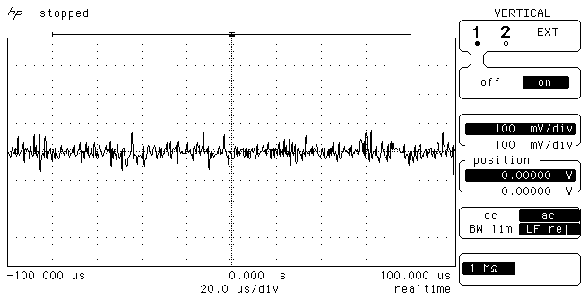
Luckily the LCD provides a signal that they often call ‘Tearing Effect’ (TE). TE goes active during a part of the display known as the ‘vertical blanking period’ which is a few lines at the top and bottom of the panel that you can’t see.

To achieve a flicker-free display we need to start refreshing data when TE goes active and we must move at least as fast as the display refresh so that it doesn’t catch us up before all the data has been uploaded.

The timing here is a critical part of the design. The LCD controller must offer a write speed that allows a complete frame to be written in less time than the display refresh rate and our graphics accelerator must be able to write data out at that speed.
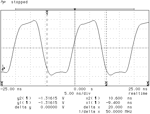
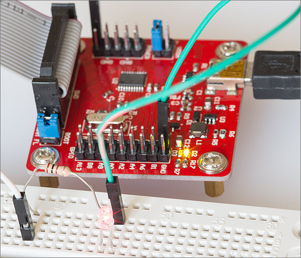


Click for larger

The screenshot shows the TE signal from the LCD used in this project captured using my Ant18e logic analyser.

High level components

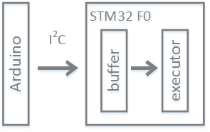
It’s not possible to do all of this using an unassisted MCU with CPU power alone. We need to offload the heavy lifting involved with moving all those graphics around to a co-processor and as you can tell from the title of this article I’ve elected to use an FPGA to do that. Why an FPGA? The core of this graphics accelerator involves interacting with external components at high frequencies and with nanosecond-level timing margins. The amount of combinatorial logic involved is fairly low and so an FPGA is the obvious choice.

The FPGA will not be the only processor on this board. Games need a controller, and it needs to be a pretty decent one if we want to be able to perform game-engine computations in the fixed period available to us between frames. I’ve elected to include the MCU on-board instead of just breaking out the FPGA interface to a pin header because parallel buses and high signal frequencies will not play well with flying interconnect wires.

Games need graphics, lots of graphics. To deal with that I’m going to provide an SD card slot that the controller can use to access graphics and other data authored on a computer. The FPGA isn’t going to be talking to the SD card because SDIO does not offer a predictable, constant sustained transfer rate so I’ll provide a high-capacity flash memory IC that the FPGA can use to read the graphics at high speed.

The FPGA needs a RAM buffer to render its frames to. FPGAs do come with some different types of very fast RAM on board but it’s nowhere near large enough for a frame buffer so we’ll need to add a chunk of our own. Asynchronous Static RAM (SRAM) offers the simplest interface and the possibility of high sequential throughput so we’ll use it in preference to SDRAM. The other option, SDRAM, is cheaper and offers densities far in excess of what we need but the controller is much more complex and does not deliver a benefit in this design.

Of course we also need an LCD to display the actual image and I’m going to choose the highest resolution device that I can possibly get away with given the space and time constraints imposed by the other resources.

As a final touch I’ll throw in an EEPROM to allow a relatively small amount of data to be persisted while the power’s off. High score tables are an example of such data.

Now let’s look at a block diagram that illustrates what I’ve just talked myself into.

Component selection

Now that the basic system design has been decided, it’s time to choose the actual components that will be used on this board.
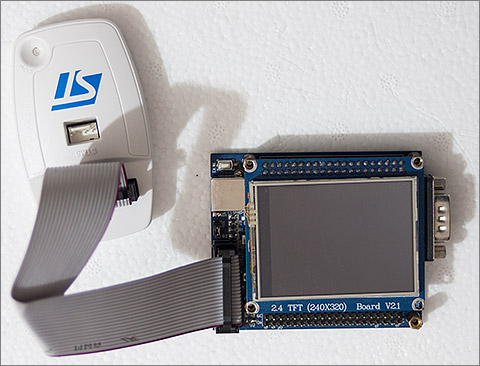
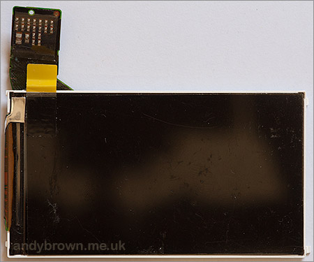
The LCD


The 3.2″ Sony Vivaz LCD

Just like in my previous project, the halogen reflow oven, I’ve selected the 640×360 LCD from the Sony Vivaz U5 cellphone. You can read all about my initial reverse engineering effort for this display in this article.

This display ticks all the important boxes for this project. Good quality replacement parts are cheaply available on ebay, I’ve worked with it before and I know it’s reliable, and the timings and resolution fit perfectly.

I’ll be driving the display in 16-bit 5-6-5 RGB mode which means I need 2 bytes per pixel. That means the frame buffer is going to have to be at least a 4 megabit SRAM part. If the resolution were any higher then it would push me into an expensive 8 megabit part and in all likelihood the timing would be too tight to achieve in the selected FPGA, again pushing up the cost and complexity into undesirable territory.
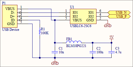
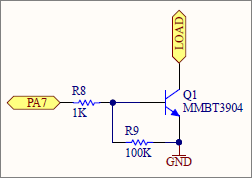
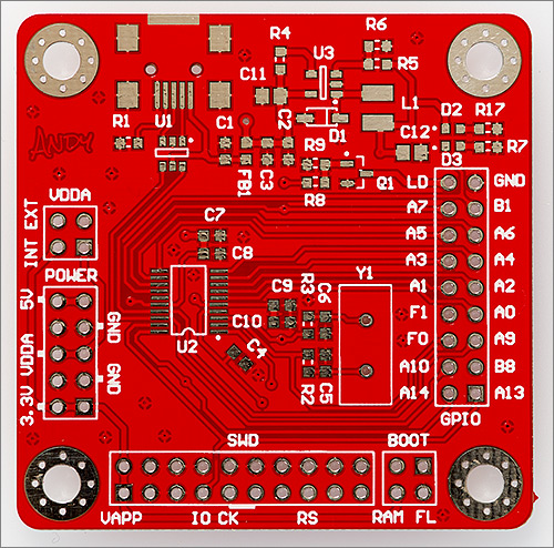
The latch

This is a small part with a critical task. If I’m going to squeeze my design into the limit of 63 FPGA user IOs then I need to take steps to reduce the pin count wherever I can. The 8-bit latch will be used to reduce the pins required by the LCD data bus from 16 to 9 (1 extra pin is required for the ALE signal).

The performance of the latch is critical to the success of the design. My timing constraints are such that the ALE line will be high for only 10ns give or take some skew so I needed to select a part that met the criteria. The Texas Instruments SN74ABT573APW device fits the bill perfectly, requiring only a 3.3ns high pulse. Not only is it fast enough but it has a sensible pinout where the outputs are on opposite sides of the device to the inputs which is perfect for a bus. Quite a lot of multi-bit latches have a crazy pinout where outputs are adjacent to the inputs which guarantees you a mess of vias as you try to reassemble your bus lines on the PCB.
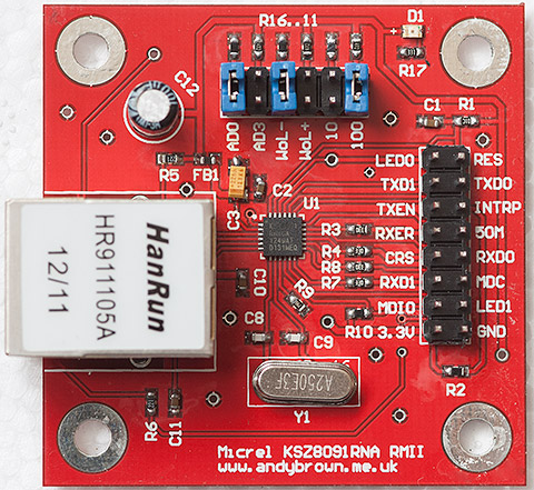
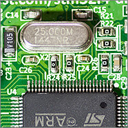
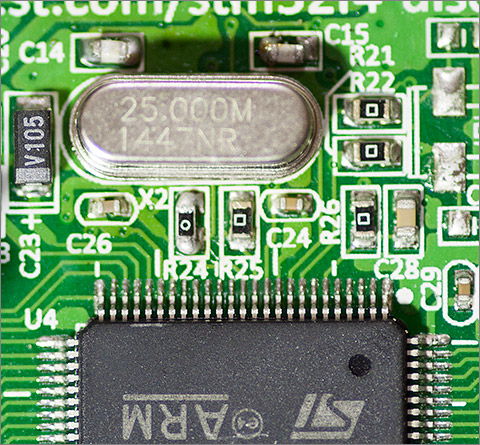
The FPGA

I chose the Xilinx Spartan 3 XC3S50 in the -5 high speed grade as the FPGA that I would use. This is the smallest, cheapest and most hobbyist-friendly Xilinx FPGA in production and it’s still got 100 pins, somewhat validating the FPGA’s reputation as being big, formidable devices to work with. At least it’s not a BGA is all I can say.

The top two manufacturers in the FPGA market are Xilinx and Altera. Xilinx was first off the block in the FPGA industry and has the lion’s share of the market. My choice of Xilinx over Altera is based on local availability of the parts. Farnell UK is a Xilinx supplier and so it made sense for me to choose Xilinx. Both manufacturers offer free synthesis and simulation software and a similar product line-up so if Altera parts are easier to find in your locality then I’m sure you’ll get by just fine with Altera FPGAs.

Back to the XC3S50. It’s quoted as having 50,000 logic gates but that’s an aggregate number that isn’t really reflected in the resource usage you see when you synthesise your design. The key figures are that it has 1,536 slice flip-flops, 768 slices and 1,536 4-input LUTs.

As well as the core logic gates there are some additional on-chip resources that are going to be crucial to my design. There are 73,728 bits of dual port block RAM (BRAM), 12,228 bits of distributed RAM, 4 hardware multipliers and 2 digital clock managers (DCM).

It’s important to note that the distributed RAM is not an independent resource like the block RAM. Distributed RAM is implemented using LUTs, reducing the area available to hold your design logic.

I will use the BRAM to hold the sprite records, the distributed ram to implement a FIFO for incoming commands from the MCU and a DCM to synthesize a high frequency clock from an external oscillator.

Of those 100 pins, 63 are available for user IO. That might seem like a lot but once you start adding up the SRAM address and data buses, the MCU interface and the LCD bus it doesn’t look so generous after all. You’ll see how I squeeze it all in as you read the rest of this article.

Finally, do you see that huge bump up the top right of the package that looks like it ought to be the pin 1 indicator? Well it’s not. Pin 1 is down at the bottom left next to the much smaller bump. I found that one out the hard way. The convention with ICs is that if you hold them with the printed text upright then pin 1 will be at the bottom left.
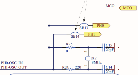
The oscillator

If you want to do anything significant in an FPGA then you need to supply it with a clock signal from an oscillator. A cheap quartz crystal isn’t sufficient, it must be a full oscillator. These cost slightly more but are still very affordable.

The oscillator I chose is the 40MHz Fox FXO-HC73 and it will be fed to one of the global clock pins on the FPGA. FPGAs provide dedicated low-skew routing resources for clock signals to ensure that all the parts of your design that run off the clock are closely synchronised.

The entire FPGA design runs at 100MHz so I use one of the DCM resources inside the FPGA to multiply up the 40MHz signal to 100MHz. There’s no critical reason to choose 40MHz for the oscillator, it’s just one of the cheaply available frequencies that multiplies/divides to 100MHz easily and isn’t too fast to cause routing problems on the PCB.
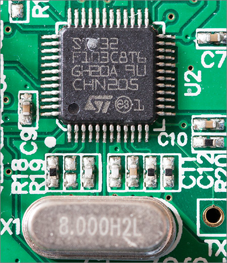
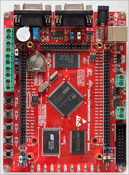
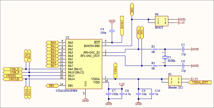
The MCU

The MCU is going to be the STM32F429VIT6. It’s a 180MHz 32-bit ARM Cortex M4 MCU from ST Microelectronics that comes with 2Mb of flash memory, 256Kb of SRAM and a hardware FPU capable of single-cycle add and multiply operations on single-precision floating point numbers.

It’s a formidable MCU and I chose it because of its high core clock speed and abundant resources. All the game logic has to execute in a fixed time period so it pays to have a high clock speed. It’s almost certainly overkill, and the fact that the F429 contains a ‘Chrome-ART’ accelerator that has considerable functional overlap with the sprite accelerator has not gone un-noticed. However I decided to err on the safe side and fit the fastest STM32 currently available.

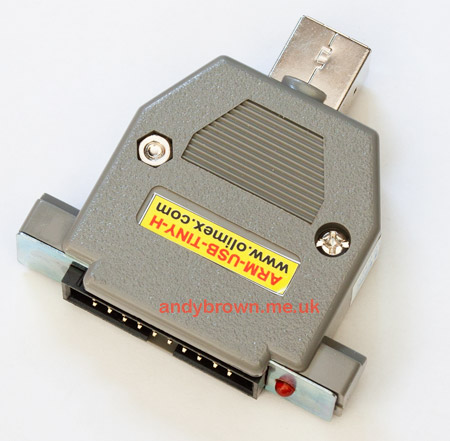
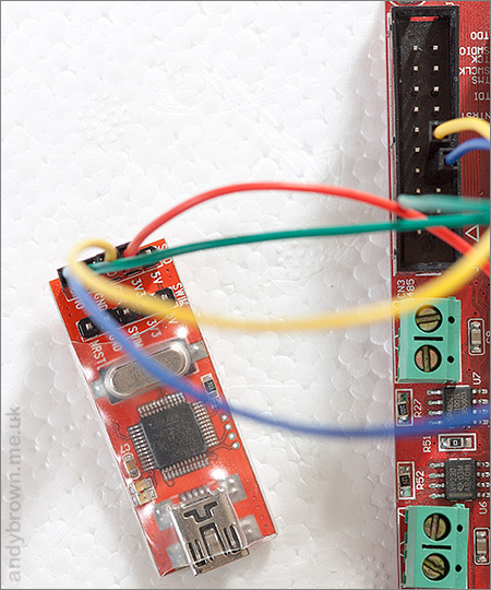
Programming the device is easy, all I need to do is expose the SWD pins, connect up my ST-Link/v2 programmer and I can program it using OpenOCD.

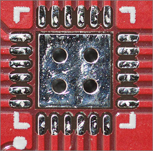
The MCU is available in a number of packages with the LQFP-100 being the one with the fewest number of pins. Not exactly small but there’s already a quad 100 pin package on this board so what’s another one between friends?

The flash

The flash device is a 128 megabit (16 megabyte) S25FL127S SPI part from Spansion. This device was selected for its low cost, high speed and high capacity. Uncompressed graphics require lots of space and multi-frame sprites only multiply up that space requirement. This device has the capacity for 8 megapixels, or 36 complete full frames of data.

If you think SPI flash is not going to be fast enough then you’re going to be pleasantly surprised. The Spansion device can operate in a non-standard 4-bit output mode and can be clocked as high as 108MHz giving a maximum data output rate of 54 megabytes per second. Operating this kind of bus is bread and butter to an FPGA. I’ll clock the flash device at the full internal FPGA clock speed of 100MHz and I’ll use the 4-bit quad output mode to enable me to read out a 16-bit pixel in 4×10 = 40ns. This just happens to be exactly how long I need to write out a pixel to the SRAM frame buffer. Serendipitous indeed.

The SRAM

The SRAM IC that I chose is the ISSI IS61LV5128AL 4Mb device arranged in a 512Kb x 8-bit layout with an access time of 10ns (100MHz). The LCD pixels are 16-bits wide so I’ll need to do two SRAM accesses to read or write a full pixel but I’ll save 8 pins from my FPGA budget.

4 megabits is enough to hold 262,144 pixels. My LCD has 640×360 = 230,400 pixels so there’s 31,744 to spare. I don’t have a use case for those extra bits so they’re just going to be left unused in this design.

The 10ns access time means that I’ll have no trouble doing a full pixel write in the same time frame that a 16-bit pixel is read out from the flash IC. Conversely, I’ll be able to read out a full pixel in the same time period that it takes to write out a pixel to the LCD. FPGAs are designed to do multiple tasks concurrently with nanosecond precision so everything should line up nicely.

The EEPROM

The EEPROM plays a peripheral, non-core role in the design. It’s just there so that we’ve got some space to store arbitrary data that must survive a power-cycle. Unlike the popular Atmel AVR chips used in the Arduino, the STM32 MCUs do not come with EEPROM built-in. It’s possible to write flash-pages inside the STM32 on-demand so EEPROM can be emulated but with the cost of I2C EEPROMs so low I figured I might as well include one here.

The device I chose is a 32Kbit BR24G32FJ device from Rohm in the SOIC-8 package.

EEPROMs are a rare example where there is cross-manufacturer pinout and operational compatibility. You can pretty much choose any device in the right-sized package and it’ll work over the I2C protocol just the same as a device from a different manufacturer. If you’re building this project yourself then feel free to substitute an alternative part if the Rohm device is not available where you live.
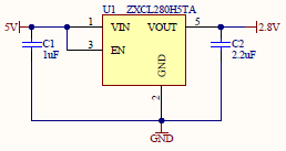
The power supplies

There are no fewer than five different levels on this board, six if you count the output from the LCD backlight boost converter. A 5V external power supply feeds the LDO regulators that supply power to the rest of the system. Nearly all the components are powered off an AMS1117 3.3V regulator except, predictably, the FPGA. It requires 2.5V and 1.2V for its auxiliary and internal operations in addition to the 3.3V level that we use for all the IOs. The last level is the 2.8V required for the LCD panel supply.

When running in sprite mode with the LCD backlight at 90% the system will draw nearly 400mA down the 5V line. For this reason I chose 3.3V, 2.5V and 1.2V regulators that have a big margin in the amount of current that they can supply. I didn’t want to be left with an iffy power supply at the end of the day. The 2.5V and 1.2V regulators are both from the Taiwan Semiconductor TS1117 family and the 2.8V regulator is the ZXCL280H5TA by Diodes Inc.

It’s all about the timing

All of the selected components must work together within the timing constraints imposed by how fast we can get data out of the flash IC, into the SRAM frame buffer and subsequently to drive into the LCD. Here’s a diagram that shows a high level overview of the timing from the point of view of the game developer.

At the start of the first frame the FPGA will drive a busy signal high to indicate that it’s about to start parsing the sprite configuration stored in the internal BRAM. It will use this configuration to fetch graphics from the external flash and write them out to the SRAM frame buffer. During this period it is not safe to write any commands to the FPGA that would cause the sprite state to change.

When the FPGA has finished this task it will drive the busy signal low again. This transition must happen before the start of the next frame or display corruption will be observed. The MCU should use this period to run its game logic and prepare for writing out the new state of the display.

During the second frame the FPGA takes the data in the frame buffer and writes it out to the LCD as a complete frame. During this period it is safe for the MCU to upload the new state of the world to the FPGA. In fact it’s safe to do so as soon as the busy signal goes low.

When frame two is complete the whole cycle starts back again at frame one. Since the display is running at 60fps what we’ve got here is a 30fps sprite engine.

More about the sprites

I’m planning to provide two operating modes for the FPGA. In passthrough mode the FPGA will send data that it receives from the MCU directly through to the LCD bus. This allows the MCU to directly drive the embedded Renesas R61523 controller in the LCD at a decent speed but not as fast as if it were directly connected. This mode is used to initialise the LCD controller, display introduction and high score screens and to send the command sequence that prepares it for entering sprite mode.

In sprite mode the FPGA takes over driving data to the display as described in the above timing diagram. The MCU can only send sprite-related load/move/show/hide commands. The FPGA requires a 127-bit record to hold the full state of a sprite and the BRAM address bus width must be a power of 2 therefore we can store a total of 512 sprites in the FPGA, where one sprite equals one graphic or one animation cel. That should be more than enough for a game and in fact I’ll find that I’m limited by timing more than anything else.

To show a complete frame the sprites must occupy 100% of the pixels on the display. There is no fill background command so the background must be made up of one or more sprites that cover the entire frame. If a solid colour background is required then a solid colour sprite must be provided for that purpose. The FPGA design provides the facility to auto-repeat a sprite in the X and Y directions to help optimise both flash and sprite memory usage.

Sprites are arranged so that the first one is at the back and the last one is at the front. Pixel transparency (but not alpha level) is provided so that sprites can be an irregular shape or have cut-outs within them.

The last feature that I’m providing is a partial display model. This allows me to define which sprite data row and/or column should be the first to be displayed and which should be the last. Rows/columns outside the range are ignored during the display writing phase.

In the above picture, sprite 4 has its ending column set so that it appears to be hanging off the right edge of the display. Sprite 5 has its starting column and ending row set so that it appears to be partially off the bottom left of the display.

In practice this feature is used to allow sprites to ‘walk on’ and ‘walk off’ the edges of the screen, or it can be used to achieve smooth omni-directional scrolling. I plan to put both of these features to the test in my game demonstration.

Limiting factors

The limiting factor that governs how many sprites I can display is the LCD frame timing. The rendering of the sprites into the frame buffer by the FPGA must finish within one frame, or 16.2ms. Let’s see how that timing budget can be spent.

The FPGA will check every one of the 512 sprites to see if it needs to display it or not. It takes 30ns to check each sprite giving us a fixed overhead of 30 x 512 = 0.015ms. So small that it can be considered negligible.

For each visible sprite, there is a constant setup and completion time of 280ns. This applies even if a sprite is being auto-repeated in the X or Y direction by the FPGA. For each pixel there is an overhead of 40ns. So we end up with a formula of ((40 x num_pixels) + 280)/1,000,000 ms per sprite. This is the important calculation.

In a game where the display has a solid colour background then we have a fixed overhead for it of ((40 x 640 x 360) + 280)/1,000,000 = 9.21ms. That leaves us 6.99ms for sprites that represent the game action. If we re-arrange the timing formula to work out how many pixels that leaves us then we come out with around 174,000, or to put it another way about 75% of the display area. That is the limiting factor for any game design and it’s something I’ll need to bear in mind.
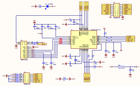
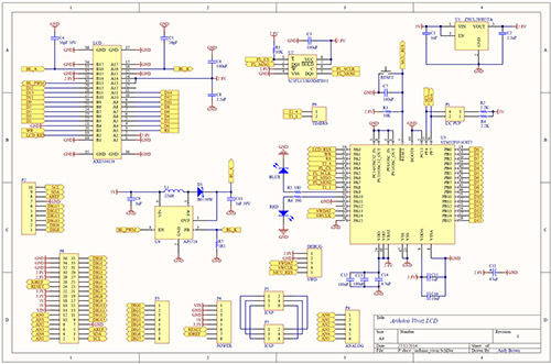
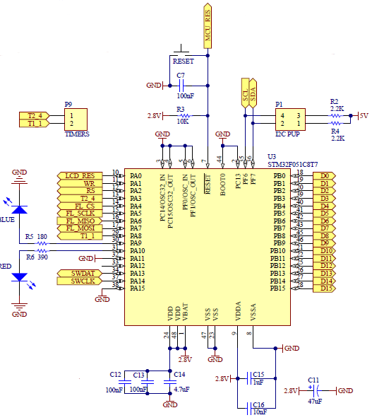
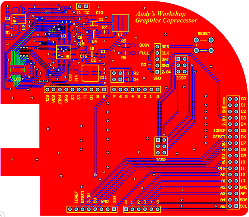
The schematic

Now that I know the parts I’m going to use I’m going to create the schematic that links them all together. Click on the thumbnail to view a full-size PDF of this design.


Click on the thumbnail for a PDF

As you can see it’s quite a large one and is predictably dominated by the FPGA and the MCU. It’s much easier to follow if we break it down into modules. Let’s do that now.

The power supply

Inputs to the main trio of regulators comes into a jack plug from an external 5V supply. The 2.8V supply is located physically far from the 5V input so it was more convenient to supply it from the 3.3V power line. The 10µF and 22µF smoothing capacitors are all tantalum and are all placed physically very close to the regulator that they are designed to work with.

C26, C18 and C23 are electrolytics that provide bulk low-frequency decoupling for the board. In one of Xilinx’s many design guides they recommend that every decade up to 100µF is covered by decoupling so I’m sticking to that recommendation here.

The 120Ω resistor from the 2.5V line to ground is another Xilinx feature. In XAPP453 Xilinx explain how to configure (program) an FPGA using a 3.3V MCU. One of the steps that must be taken is to include the 120Ω shunt resistor from 2.5V to ground to prevent the regulator from seeing a reverse current on its output pin. The downside of this requirement is that there will be a constant 20.8mA (50mW) drain even when nothing is happening.

It pays to study the thermal characteristics part of the voltage regulator datasheet. In my early experiments I was running this design with a 12V input instead of 5V. After running for some time I noticed that the system was spontaneously resetting itself. Odd, I thought, and then I touched the board. It was red hot around the AMS1117. The AMS1117 was going into thermal shutdown to protect itself from burnout and I went back to the datasheet to find out why.

In the thermal considerations section of the datasheet the formula for the power dissipation is given as PD = ( VIN – VOUT )( IOUT ). For my 12V input with a 400mA worst-case output that’s 3.48W of heat that’s going to be generated. Rather a lot. Going on to plug that figure into the formula for the maximum junction temperature gave me a figure of 233°C. The maximum allowed is 125°C. Hardly surprising that I was running into issues. By reducing the input voltage to 5V the power dissipation drops to a mere 0.68W and the maximum junction temperature to 65°C. Much better, and a valuable lesson learned.
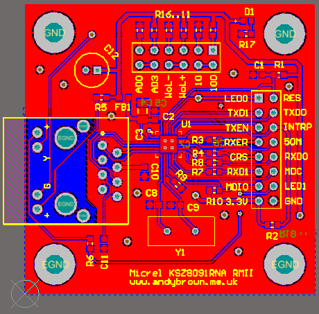
The FPGA

The FPGA is pictured here with its decoupling capacitors not shown to save space. If you want to see the decoupling network then please view the full PDF. The decoupling for the FPGA is quite substantial and attempts to follow the guidelines in Xilinx’s Power Distribution System (PDS) Design application note.

I’m using 62 out of the 63 available IOs in this design, only just squeezing in everything that I need. I chose the FPGA pins to be friendly to the ICs such as the SRAM, flash and the latch. The idea is that the components with high frequency signals will be placed very close to the FPGA and should require no board vias. This is meant to be a hobbyist-friendly design so it’ll be a 2 layer board and that means I must take care with the signal routing.

The SRAM is the greediest IC, requiring 28 IOs to cover its address, data and WE control signals. I’m saving 2 pins here by tying CS and OE both to ground as permitted in the SRAM datasheet.

The flash, being a SPI device is quite frugal in pin usage requiring only 6 pins in total. I can’t tie CS low with this device because CS is used in the SPI protocol to terminate certain command sequences.

The signal inputs from the MCU are the 10-bit data bus D0..9, the WR strobe and an active-high reset. The outputs to the MCU are the busy signal and a debug output that I used during development to set when certain states occurred. Debugging an FPGA in-circuit is about as hard as it gets folks.

All the programming signals, PROG_B, INIT_B, CCLK, DIN and DONE are all present and correct. I will be programming the FPGA using what Xilinx calls slave serial mode where an MCU clocks data into the FPGA and monitors the output signals to determine the success of the operation. The compiled .bit design is about 55Kbytes in size and takes a few tenths of a second to upload from the MCU.

I compile the .bit file in with the MCU program and load it into the FPGA on startup. For those that don’t know, an FPGA configuration is held internally in volatile SRAM so it’s lost when the power goes off and must be restored on system startup. (Some FPGAs do come with internal configuration storage flash memory but this family does not).

The LCD signals include the 8 bit data bus, the latch control line (LE) and the RS and WR lines. Going the other direction is the vital TE signal that will allow us to synchronise to the LCD frame output.

VCCO[0..7] are the 3.3V inputs, there’s one per FPGA IO bank. VCCINT are the 1.2V inputs and VCCAUX are the 2.5V inputs. This is a lot of power pins and associated decoupling capacitors and it only gets worse as you go up to larger FPGA packages. Another reason to stick with the small devices for hobbyist designs.
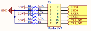
The MCU

The MCU is the counterparty to the FPGA in this design and you can easily see the opposing ends of some of the signals. For example I map the whole 10 bit data bus and the WR signal to port E. This will allow me to set the data and the WR strobe in a single port write. A reset button is provided just in case I need to externally reset the board at any time.

The SDIO signals map to the pins connected to the MCU’s SDIO peripheral so I can read and write to the SD card easily. The I2C SCL and SDA lines are connected to the I2C#2 peripheral inside the MCU and I’ve elected to provide two LEDs for status and other general purpose use. 18 of the GPIO pins are broken out to an external pin header so that I can add peripherals such as joysticks and other input devices for testing. The pins that are broken out are not done so at random, they are selected to cover a variety of the onboard peripherals that could be useful during development.

You may notice that that there’s no oscillator or quartz and that’s because this MCU doesn’t need one. As long as you can make do with 1% clock accuracy then you can use the internal 16MHz High Speed Internal (HSI) oscillator as the input to the PLL that generates the 180MHz core clock. 1% is fine by me and so I use the HSI.

After the complex requirements of the FPGA, the power supply for the MCU is a breath of fresh air. Decoupling (not shown in the screenshot) follows ST’s guidelines of a ceramic capacitor per-pin and a 4.7µF ‘chemical capacitor’ on the board. Electrolytics are chemical capacitors so that’s what I used. I prefer tantalums for their low ESR but didn’t have any to hand at the time.

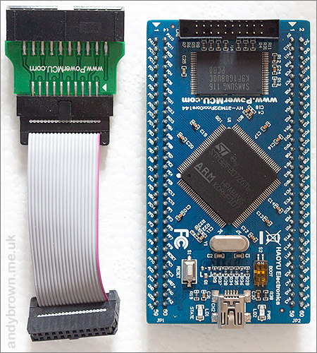
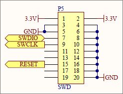
Debugging and programming is done using SWD, a two wire protocol designed to replace JTAG as a more efficient design. SWDIO and SWCLK are broken out to a debug header on the board that can be directly connected to the cheap and effective ST-Link/v2 programming dongle.
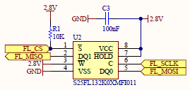
The flash

The flash IC is the highest speed external peripheral on this board. The clock will run at 100MHz which is well into the territory where I could have signal integrity issues caused by overshoot, undershoot, reflections or any combination of the above if I’m not careful. For that reason all of the IO lines and the clock all feature 33Ω series termination resistors designed to sink reflections before they can harm the signal. These lines will also be kept very short on the PCB.

How did I decide on 33Ω? Rule of thumb I’m afraid. I don’t have the kind of equipment required to measure and select an ideal value so I’m starting at 33Ω and if I get problems then I’ll break out my bench oscilloscope and see whether I need to increase the resistance or not.

The SRAM

Memory ICs are not very exciting really. They’re just a pair of buses, a few control strobes and the power supply. To save on pins I’m connecting CS and OE directly to ground as permitted by the datasheet. I just need to control WE when I need to write data.

The address and data lines will change at a maximum of 50MHz in this design but the WE line will toggle at 100MHz. I’m not concerned about the address and data as long as I keep the lines short and without vias then 50MHz won’t be a problem. Writing this after the fact I do think that I should have at least put a footprint in for a 33Ω resistor on the WE line. If and when I produce another revision of the board then I think I’ll do just that.

The oscillator

An oscillator doesn’t need to be kickstarted by an external device and will start ticking from the moment it’s powered up. In my design I’ve elected to include a 33Ω series termination resistor on the clock line even though it’s probably overkill. This clock is so critical to everything else that I thought I’d be better safe than sorry.
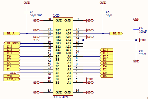
The LCD

The schematic for the LCD will be familiar to anyone that’s read either of my reverse engineering or my halogen reflow oven articles.

All of the control signals are connected to the FPGA except LCD_RES which is the reset signal. This one is connected to the MCU. There’s no need for us to bother the FPGA with the burden of the LCD reset sequence, this is best performed by the MCU.

The LCD backlight

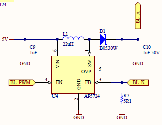
The backlight for this LCD consists of six white LEDS in series so we need a boost converter to generate the high voltage required to overcome the combined voltage drop of each LED.

The AP5724 from Diodes Inc. is a dedicated current-mode backlight driver that incorporates a boost converter. You only need to add a few external components including a current-setting resistor and the driver will then consistently output the selected current as long as the EN pin is driven high.

The cool thing is that we don’t even need to supply a PWM signal to the EN pin to control the backlight brightness because the LCD has a function to do that for us. All we need to do is tell the R61523 controller the duty cycle that we’d like to use and it’ll do the rest. That saves us a pin and a timer resource on the MCU.

The latch

The latch sits between the FPGA and the LCD, allowing us to use only 8 pins on the FPGA to drive a 16 bit data bus.

When LE is high the latch is transparent, data passes through from the D inputs to the Q outputs. A few nanoseconds after LE goes low the latch goes deaf to its inputs and continues to drive its outputs from the last data that it saw on those inputs.

What we do is write out the first 8 bits of data, lock the latch and then write out the second 8 bits. As you can see from the schematic this will result in all 16-bits being driven. What’s really helpful is that the FPGA design can be coded to output any bit to any pin so I can tailor the design so that the data bus can be laid out in parallel on the PCB without any vias.

The EEPROM

The EEPROM is an I2C device that provides some persistent storage for us.

The Rohm 32 Kbit IC has a simple 2-wire I2C interface. Nothing much to say here, it’s hooked up to the I2C peripheral on the MCU. I2C is a bi-directional single-wire bus that provides protection against being accidentally driven by multiple drivers by operating in open-drain mode. That means that the bus (and clock) must have pull-up resistors somewhere. I provide those 4.7kΩ pull-ups close to the MCU as you can see in the MCU schematic.

The SD connector

An ALPS SCHD3A0100 SD card cage is provided to house a micro SD card. The cage I’ve chosen accepts a slide-in SD card which is then locked into place by sliding it back a millimetre or so underneath a lip. Once in, it’s held securely and is not likely to fall out of its own accord.

I envisage that the graphics data will be much larger than I could program into the core of the MCU so some sort of external interface is required. SD cards are the most convenient way to do that and the MCU has a built-in SDIO peripheral that will allow me to access the card in the high-speed 4-bit mode. SDIO is another bus that requires pull-ups on its data and command lines, presumably because it’s also running in open-drain mode. I provide these 10kΩ resistors in the MCU schematic screenshot.
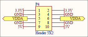
The pin headers

Two 2.54mm pin headers are provided for GPIO and debugging.

The pinout for the debug header matches the requirements published by ST Microelectronics for the SWD protocol and the ST-Link/v2 programmer/debugger. I’ve been really impressed with the ST-Link/v2. I use it all the time now with OpenOCD as the debug server and it’s never let me down.

The GPIO header breaks out a number of pins from the MCU for general purpose use. I’ve made sure that quite a few of the commonly used peripherals are covered including the I2S peripherals that I may use in the future for prototyping an audio capability.

Bill of materials

Here’s the full bill of materials for this project. There are, as you might expect, rather a lot of components. Nearly all are available at Farnell, my preferred local supplier and I’ve included links to their site where possible but you will have to venture further afield for a few of the other components.

A few of the components can be substituted for compatible devices from other manufacturers where something is available in the same footprint. Examples are U1, U2, U3, U12, L1, D1. Xilinx and ST both recommend low ESR capacitors for decoupling so choose the electrolytic and tantalum devices carefully.

Designator Value Description Footprint Quantity Farnell
C1, C2, C3, C5, C6 10µF Tantalum capacitor 1206 5 2353045
C4 22µF Tantalum capacitor 1206 1 2333013
C7, C8, C10, C13, C19, C24, C27, C28 100nF Ceramic capacitor 0402 8 1759380
C14, C21, C22, C29, C31, C32, C33, C39, C40, C41, C44, C46, C47, C49, C50, C58, C59, C60 100nF Ceramic capacitor 0603 26 2211177
C9, C12 10µF Ceramic capacitor 0805 2 2320852
C11, C15, C34, C38 1µF Ceramic capacitor 0603 4 1759399
C16 56pF 50V Ceramic capacitor 0603 1 1759063
C17 56pF Ceramic capacitor 0603 1 1759063
C18 100µF Electrolytic capacitor radial 2mm 1 8767122
C20, C25, C36 10nF Ceramic capacitor 0603 3 1759022
C23 47µF Electrolytic capacitor radial 2mm 1 2079293
C26 4.7µF Electrolytic capacitor radial 2mm 1 1236668
C35 1µF 50V Ceramic capacitor 0805 1 1845750
C37, C45, C48 2.2µF Ceramic capacitor 0603 3 1759392
C42 4.7µF Ceramic capacitor 0603 1 2320811
D1 B0530W Any compatible schottky SOD123 1 1863142
DEBUG HDR2X10 Header, 10-Pin, Dual row 2.54mm 1
L1 22µH Inductor 6x6x3mm 1 1864120
LCD AXE534124 Panasonic connector (Digikey US) 17x2x0.4mm 1
LED2 Blue LED LED, <3.3V Vf 1206 1 2322084
LED3 White LED LED,<3.3V Vf 1206 1
P1 HDR2X11 Header, 11-Pin, Dual row 2.54mm 1
P2 SCHD3A0100 ALPS Micro SD connector 2.54mm 1
P3 2.1mm PCB power jack 1 2.1mm
POWER Red LED Power indicator 1206 1 2099256
R1 120Ω Resistor 0603 1 2331714
R2, R20, R21 390Ω Resistor 0805 3 2331790
R3, R23, R24 4.7KΩ Resistor 0603 3 1469807
R4, R7 68Ω Resistor 0805 2 2138823
R5 330Ω Resistor 0603 1 2331721
R6 5.1Ω 1% Feedback resistor 0805 1 2128935
R8, R9, R14, R17, R22, R26, R27, R28, R29 10KΩ Resistor 0603 9 9238603
R10, R11, R12, R13, R16, R18 33Ω Resistor 0603 6 9238301
R25 1KΩ Resistor 0603 1 2073348
RESET PCB Button Make type 1
U1 TS1117BCP 1.2V LDO regulator TO-252 1 1476674
U2 AP1117E33G 3.3V LDO regulator SOT-223 1 1825291
U3 TS1117CW 2.5V LDO regulator SOT-223 1 7208340
U4 SN74ABT573APW Octal latch TSSOP-20 1 1740911
U5 XC3S50 Xilinx Spartan 3 FPGA VQ100 1
U6 IS61LV5128AL ISSI 512K x 8 10ns SRAM TSOP2-44 1 1077676
U7 AP5724 Diodes Inc. LED driver SOT26A-6 1
U8 ZXCL280H5T Diodes Inc. 2.8V LDO regulator SOT353-5N 1 1461559
U10 S25FL127S Spansion 128Mb serial flash SOIC8 (208 mil) 1 2328002
U11 STM32F429VIT6 STM32 F429 MCU LQFP100 1 2393659
U12 BR24G32FJ Rohm 32Kb I2C EEPROM SOP8 1 2373743
X1 FXO-HC375 Fox 40MHz SMD oscillator 1 custom 1641011

PCB design

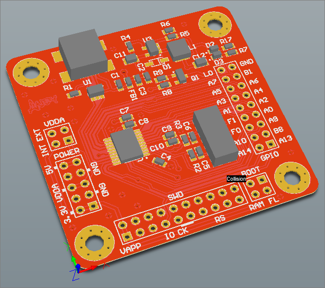
I decided to target a low-cost 2-layer 10x10cm board of the sort that any hobbyist can afford to have printed at one of the Chinese prototyping houses. Routing it took a while. A long while.

The first component to go down was the LCD connector because it must physically sit in a specific place so that the LCD can be mounted on to the board in a position that allows the other connectors to be placed around it. The LCD connector is actually on the bottom of the board which, when sitting on my desk is facing upwards.

The next component to go down is the FPGA which I plonked down close to the center but mindful that I’d need to place another 100 pin device not far away.

After the FPGA the flash and the SRAM are placed as physically close to the FPGA as I dare and their IO traces are routed carefully.

Next to be routed are the FPGA power and decoupling traces. These traces are wider than most and the ceramic decoupling capacitors are placed as close to the FPGA pins as I can put them, and that meant using very small 0402 components for some of the pins. Others are decoupled on the opposite side of the board and use larger 0603 and 0805 packages.

Now that the components with specific requirements are down it was just a matter of placing the MCU in the best position I could find and routing the remaining signals. That part was not hard, just time consuming.

Final touches include a silk-screen logo, M3 mounting holes and some cool looking rounded corners on the PCB as a whole. The mounting holes are actually quite important because this board will be operated component-side down I will need stand-offs to provide the necessary clearance.

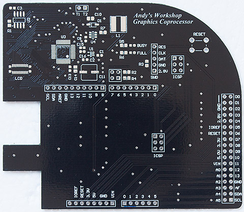
Let’s take a look at the routed PCB. I’ve hidden the ground pours on this screenshot to better show off the traces and components.


Click for a larger view

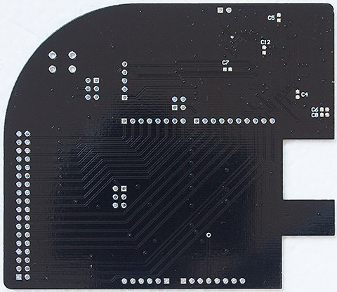
I elected to get the board printed at Elecrow, one of the many Chinese online services that’ll print you ten copies for a very reasonable price. About two or three weeks later the boards arrived in the mail and they look great!


Click for larger

Note how the all the important traces from the FPGA go directly to their target ICs as a bus with no vias. One of the many beauties of working with an FPGA is that you decide the function of each pin and if you plan ahead then you can keep your board neat and tidy.


Click for larger

I inspected a PCB under a magnifying glass and could only find one issue, which was entirely my fault. The drill holes for the 5V power supply connector were too small by about 1mm. I’d mis-entered them into the footprint designer and not spotted it during any of my post-routing visual checks. Thankfully there was an easy solution to the problem, all I had to do was shave off about a millimeter from the legs on the power connector and I would be OK.

Assembling the PCB

Putting it all together required a bit of forward planning. I wanted to reflow the majority of the components using my halogen reflow oven but the problem was that the 34 pin, 0.4mm pitch LCD connector on the other side would also need reflow.

In the end it wasn’t so hard. I zoned off the area underneath the LCD connector that thankfully only housed a few small ICs for the backlight driver and reflowed the entire remainder of the component side in my reflow oven. For the second stage I turned the board over and reflowed just the LCD connector on my hot plate by holding the PCB with just the aforementioned zoned off area over the plate.

Now I could return to the zoned off area and reflow the remaining SMD components manually with my hot air gun. Finally the easy through-hole components were soldered into place with a regular iron. After a quick bath in white spirit to clean off the flux residues she’s ready for the photoshoot.


Click for larger

That’s the component side with everything in place. The reflow process in the oven, my first major project with the halogen oven, took care of everything very well but I still went around afterwards touching up joints here and there with my iron under the microscope.
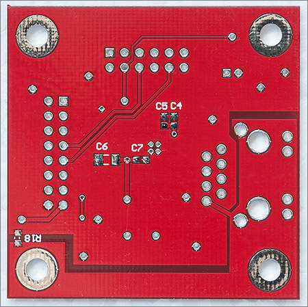


Click for larger

And the back side, which will actually be the topmost side when in use shown here before the LCD is attached. The array of decoupling capacitors that belong to the FPGA are clearly visible.


Click for larger

And the top side again, now with the LCD and 10mm standoffs in place. The LCD itself is held down and lifted clear of the PCB and the exposed capacitors with a set of double-sided sticky pads. The debug cable is shown in place, just missing that capacitor by a few millimetres (phew!).

Still with me? Great. The hardware was the easy bit, now I’m going to tackle the MCU firmware and the FPGA design. This should be fun.

Testing

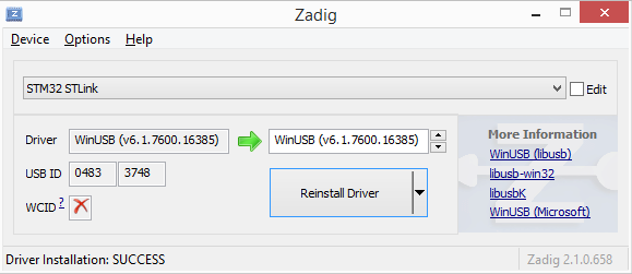
Obviously the first step in the testing phase is just to apply power, cross fingers and switch it on. The red power LED lit up. A little victory. Next we can see if the MCU’s alive by attaching the ST-Link/v2 dongle and seeing if I can connect to it with OpenOCD.

$ bin-x64/openocd-x64-0.7.0.exe -f scripts/board/stm32f4discovery.cfg
Open On-Chip Debugger 0.7.0 (2013-05-05-10:44)
Licensed under GNU GPL v2
For bug reports, read

http://openocd.sourceforge.net/doc/doxygen/bugs.html

srst_only separate srst_nogate srst_open_drain connect_deassert_srst
Info : This adapter doesn't support configurable speed
Info : STLINK v2 JTAG v17 API v2 SWIM v4 VID 0x0483 PID 0x3748
Info : Target voltage: 3.193738
Info : stm32f4x.cpu: hardware has 6 breakpoints, 4 watchpoints

As you can see I’m using the pre-canned script that sets the interface and target MCU as if it were an F4 discovery board and we have a complete success, the MCU should now be programmable.

MCU test code

I wrote a number of small test programs to check out the various features on the board and you can see them all on github. They all make use of my stm32plus library to take the heavy lifting out of working with the STM32 peripherals. Although the stm32plus library does not directly support the F42x line it’s quite OK to use the supported F40x build, you just won’t get any support for the additional peripherals on the F429.

      GpioD<DefaultDigitalOutputFeature<10,11> > pd;

      // loop forever switching it on and off with a 1 second
      // delay in between each cycle

      for(;;) {

        pd[10].reset();
        pd[11].set();
        MillisecondTimer::delay(1000);

        pd[10].set();
        pd[11].reset();
        MillisecondTimer::delay(1000);
      }

An alternate on-off blinker for the two LEDs

One small hurdle that I had to overcome was the issue of the startup code and setting the core clock to 180MHz using only the internal oscillator. After reset and before main() executes every STM32 program goes through a small routine to configure the device’s clock tree and set the speeds of the various buses.

I couldn’t find any sample ST initialisation code for the F429 using the high-speed internal (HSI) 16MHz clock as the system clock source. They do provide an Excel spreadsheet that supports the F40x devices so I took that as the starting point and adjusted the PLL multiplier accordingly to generate the 180MHz core clock. I couldn’t resist tidying up ST’s code – if you’ve ever seen any ST-authored ‘C’ code then you’ll know what I’m talking about! Click here to view the startup code on github.

/*
 * These are the key constants for setting up the PLL using 16MHz HSI as the source
 */

enum {
  VECT_TAB_OFFSET = 0,      // Vector Table base offset field. This value must be a multiple of 0x200.
  PLL_M           = 16,     // PLL_VCO = (HSE_VALUE or HSI_VALUE / PLL_M) * PLL_N
  PLL_N           = 360,
  PLL_P           = 2,      // SYSCLK = PLL_VCO / PLL_P
  PLL_Q           = 8       // USB OTG FS, SDIO and RNG Clock =  PLL_VCO / PLL_Q (note 45MHz unsuitable for USB)
};

One-by-one all the peripherals checked out fine. GPIO, EEPROM and crucially SDIO all worked without any problems. I’ve got to tell you, I was pleased at this point despite not even having looked at the FPGA yet. Talking of which…

Configuring the FPGA

Configuring an FPGA is analogous to programming an MCU. You take your compiled work and operate a manufacturer-defined protocol to get it on to the device whereupon the device is able to start doing what you intended it to do. Where FPGAs differ from MCUs is that their configuration is volatile, that is when you turn off the power it’s gone so you have to reconfigure it every time you boot up the power.

Xilinx FPGAs offer a wide range of configuration methods with excellent documentation. The method that I’ve chosen is called slave serial and it requires an external device (the MCU) to bit-bang the compiled configuration using a serial stream. Here’s an image from the Xilinx documentation that shows a potential configuration circuit, slightly modified by me to remove the JTAG pins because I’m not using those.

The only problem is that the configuration interface on the FPGA is powered by the VCCAUX 2.5V supply and the MCU is powered by the 3.3V supply. Luckily Xilinx have thought of that one and have produced another excellent reference document that tells us what we need to do to configure the FPGA safely from a 3.3V MCU.

The full meaning of the additional parts is very well explained by Xilinx but to quickly summarise, they’ve inserted some current limiting resistors and a shunt resistor next to the 2.5V regulator to drain away excess current so the regulator is prevented from seeing a potentially damaging reverse current on its output pin.

Configuration performance considerations

The compiled and uncompressed bit file for the XC3S50 is about 440096 bits give or take. The maximum speed that Xilinx allows me to operate the serial data line is 66MHz which reduces to 20MHz with compression. You can find these limits documented in the main datasheet under the specifications for FCCSER.

My design is going to almost fully utilise the FPGA so the rudimentary run-length compression supported by the FPGA is of no use to me and I’d prefer to take advantage of that 66MHz maximum clock. Theoretically I can program the FPGA in 440096/66000000*1000 = approx 7ms. In practice I have the additional overhead of shifting the bits for output and monitoring the INIT_B and DONE pins for status changes so in the end the debug build of the firmware can program the device in about half a second.

You can see the source to the configuration class here on github. It relies on the bit file being compiled into flash with the MCU program and you can see how I do that here on github.

Testing the FPGA

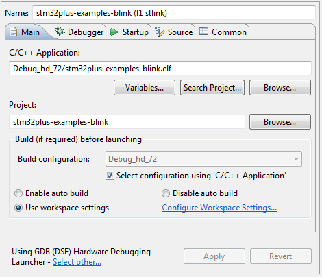
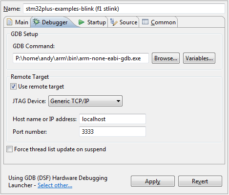
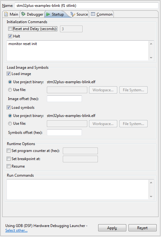
Now I have the means to configure the FPGA I need to stretch its legs a bit to check out whether my home manufacturing process has been a success. Naturally, that’s going to involve a blink test, the hardware equivalent of Hello World.

Xilinx development

Back when I decided to teach myself a hardware description language (HDL) the choice of available languages came down to two options: VHDL or Verilog. VHDL was touted as looking a bit like Pascal (ask your Dad) or Ada (ask your Grandad). Verilog was touted as looking a bit like ‘C’ (it doesn’t). I rather liked the rigorous and verbose looking syntax of VHDL and and so, since there’s no difference in the capabilities of each language, I chose VHDL. Professional FPGA engineers are likely to know both.

Xilinx offers a free development environment that they call the ISE Webpack that somehow manages to require 17Gb of space on my SSD. The tools offered by the webpack are both comprehensive and confusing in equal measure. As a beginner you’ll want to use an IDE to introduce you to the workflow and you’ll get a choice of two from Xilinx.

ISE Design Suite is the first option and the one I recommend for beginners. It appears to be written in a language that compiles to native code so it’s quite efficient and doesn’t consume many resources itself while the synthesis tools are running.

The ISE project navigator clearly shows the synthesis workflow and has an easy to use interface for creating and running simulations. It’s particularly useful for determining the availability and meaning of the many command line options that you can use.

The second option is to create your project using their Plan Ahead tool. I don’t recommend this. Plan Ahead appears to be written in java and as such it takes a heavy toll on your resources while synthesis is running. On a low powered laptop I caught it using 100% of a CPU core presumably just monitoring the tool output files for changes. However, Plan Ahead is fine for IO pin planning and is actually very useful for that task because it allows you to visualise the package while choosing pins.

I started out some time ago using ISE Design Suite and once I’d got the hang of the workflow and the command line options I dropped it in favour of a command line build environment using my favourite text editor and the scons build system. This project does not use the ISE GUI.

Xilinx command line builds

The one area where Xilinx seems to have gone completely off the rails is the ability to operate the tools from the command line in harmony with a source control system. The tools will spew literally dozens of output, intermediate and report files and subdirectories into your source directory. You can see the rules I have to create in the SConscript and .gitignore files just to hide this garbage.

Furthermore, the coregen.exe utility commits the cardinal sin of modifying its input source file when you run it making git think it’s always been modified. You have to ask yourself whether the teams that wrote these tools actually use source control themselves.

FPGA blink

Here’s an implementation of blink on the FPGA in VHDL.

library IEEE;
use IEEE.STD_LOGIC_1164.ALL;
use IEEE.numeric_std.all;
 
entity blink is
port(
  clk     : in  std_logic;
  led_out : out std_logic
);
end blink;

architecture behavioural of blink is
 constant clock_count : natural := 80000000;      -- 2x clock frequency in Hz
begin

  process(clk)
    variable count : natural range 0 to clock_count;
  begin

    -- for half the time led_out = 0 and 1 for the other half

    if rising_edge(clk) then
      if count < clock_count/2 then
        led_out <='1';
        count := count + 1;
      elsif count < clock_count then
        led_out <='0';
        count := count + 1;
      else
        count := 0;
        led_out <='1';
      end if;
    end if;
  end process; 

end behavioural;

This is a synchronous design with the sole process synchronised to the 40MHz oscillator via the clk signal. Each time the oscillator ticks a counter is increased and after a second the led_out signal is toggled.

My FPGA is not connected to an LED so I routed led_out to the DEBUG pin and used a logic analyser to verify the ticking. It worked, which told me that the FPGA was up and running, was being correctly programmed via the MCU and that at least two of the pins worked and the oscillator was ticking. A small design proved out a large part of the board.

Programming the flash

If you review the schematic you’ll see that the flash IC is only connected to the FPGA and not the MCU therefore I needed to create an FPGA design for programming it. A simple approach would have been to configure the FPGA to just pass through all signals from the MCU to the flash. The FPGA would function as little more than a buffer and all the logic would be in the MCU.

The second option would be to operate the flash programming logic from within the FPGA, accepting commands and data to be programmed from the MCU. This was the more complex option but I was up for the challenge and set about doing it this way.

The diagram shows the workflow involved in programming the flash. At a high level the MCU reads pre-formatted graphics from the SD card and then writes them one by one to the FPGA and then verifies that each one has been written correctly. The actual steps involved are:

  1. This design runs at a relatively pedestrian 40MHz so I set the non-volatile flash configuration register (CR) to the default speed setting and disable the bit that enables the quad IO mode.
  2. I issue the command to erase the entire flash device and wait for the FPGA to de-assert the BUSY pin that indicates the operation is complete. The FPGA polls the flash status register for this flag. It takes the flash about 30 seconds to complete a full erase operation.
  3. One by one I program each of the files on the SD card into the flash device by issuing block program instructions for each 256 byte page.
  4. I go back and get the FPGA to verify each of the files. I re-supply the file data for each block and the FPGA reads the block from the flash, compares it and asserts the DEBUG pin if there’s a discrepancy.
  5. I set the bits in the configuration register that enable the flash to operate at 100MHz and I enable quad output mode in the assumption that the main sprite accelerator will be the design that runs next.

The source code for all this is available on github. The MCU program is here and the FPGA design is here. I’d simulated this design before writing the MCU code so I was sure that the logic was OK and so it did more or less work first time. The only glitch I had to iron out was sampling the asynchronous WR line in the FPGA. FPGAs really don’t like asynchronous signals and you have to take extra steps to avoid metastability when sampling an asynchronous pin.


Click for larger

I really can’t emphasize enough how hard it is to debug an FPGA in-circuit so it’s imperative that designs are thoroughly simulated up-front. My in-circuit debugger consists of a single output pin that I can set or reset depending on some internal state.

The main design

The main VHDL design is broken down into components linked together by their input and output signals. In FPGA lingo they call this a hierarchical design and if you’re accustomed to any modern programming language it’ll feel completely natural to you as opposed to dumping the whole design into one file (yes, they do that too).

main is the overall container that declares the I/O port that maps directly to the pins on the VQ100 package. Main is responsible for instantiating the rest of the components and linking together their inputs and outputs. Let’s take a brief look at the purpose of each component.

mcu_interface

The FPGA is connected to the MCU via a 10-bit data bus and an asynchronous WR strobe. The MCU writes data on to this bus and then pulses WR low and then high again. The FPGA reacts to the rising edge of WR by writing the 10-bit value into an internal 64-entry FIFO implemented in distributed RAM.

At the same time, mcu_interface is also reading data off the other end of the FIFO and when it’s read enough parameters to execute the desired command it will spend a few 10ns cycles executing that command before returning to reading more data off the FIFO.

It’s up to the MCU to ensure that it doesn’t write data to the FIFO faster than the FPGA can read it off. In practice this is not likely as the MCU is likely to have to spend some time executing logic between each command during which time the FPGA will be draining the FIFO and executing commands.

The actual commands that I’ve implemented allow the MCU to write raw data to the LCD in passthrough mode, put the FPGA into sprite mode and execute commands to load, move hide and show sprites. You can see the documentation for the commands here on github.

sprite_writer

This is the big one. sprite_writer is responsible for reading sprite definitions from the internal block RAM (BRAM), reading the graphics from the flash IC and writing them to the correct locaton in the SRAM frame buffer.

The outer loop of this component iterates through each of the 512 sprite definitions acting on each one that has the visible bit set to true. For each visible sprite there are then two inner loops that handle the X and Y repetition counters that allow a sprite to be output into a grid pattern on the display.

Inside the X/Y repetition counter there is the main loop that reads data from the flash and writes it to the SRAM. This is the timing-critical part as there are only 4 cycles (40ns) available to completely process each pixel. The loop operates a sort of pipeline where each iteration writes out the previously read pixel to the SRAM while simultaneously reading the next pixel from the flash. Pixel transparency is handled and the internal logic that allows sprites to be partially visible is taken care of.

sprite_writer instantiates a couple of internal components for its own use. Those with a conventional programming background may find it surprising that the things they take for granted such as addition, subtraction and even counting do not necessarily come for free with an FPGA. If you want to add two numbers then you’ll need to implement an adder. Want to multiply? That’ll cost you a multiplier. In these days of virtual machines and interpreted languages it’s refreshing to know that little has changed at the fundamental level since I started a long time ago.

This has not gone un-noticed by the FPGA manufacturers who in many models offer hard implementations of adders and multipliers (sometimes touted as DSP primitives) distributed throughout the chip fabric. The adders that I instantiate are pipelined implementations that take less of a chunk out of my timing budget than those that xst infers if I just use the VHDL + operator.

The memorably named OFDDRSSE component is one of a family of OFDDR primitives that allow you to output a clock to an IOB (a package pin). You might think that you can just hook up an internal clock signal to an output, or maybe gate a clock with some internal logic and output that signal to an IOB. That would be naiive because it would create a high level of skew between the output clock and your design. Clocks in an FPGA are treated like royalty and there’s always a correct way to do the common clock operations. Using an OFDDR primitive is the correct way to output a clock signal to a pin and I use it to create the 100MHz flash clock with the CE clock-enable input used to switch the clock on and off.

frame_counter

In the initial design I explained how I was going to use even frames to write data from the SRAM to the LCD and odd frames to load up the SRAM from the flash. frame_counter monitors the LCD TE signal and each time it spots a rising edge it flips the bit that indicates odd or even frames.

TE is an asynchronous signal so a simple shift register is used to sample the current state and use the two previous states to check for sure if there has been a rising edge.

lcd_sender

lcd_sender is a utility component that outputs a 16-bit value to the LCD data bus, taking care of the interaction with the latch and the correct timing for the LCD WR strobe. I call it from mcu_interface when the design is in passthrough mode and I need to write out a value from the MCU to the LCD. It takes exactly 70ns to execute and has a ‘busy’ output signal and a ‘go’ input signal to allow synchronisation with its operation.

sprite_memory

sprite_memory is an instantiation of the Xilinx BRAM IP core. Block RAM on this FPGA is a true dual-port RAM with configurable data and address bus widths. I use it to store sprite definitions. Here’s the definition of a sprite record:

  -- subtypes for the various bit vectors
  
  subtype bram_data_t       is std_logic_vector(126 downto 0);
  subtype sprite_number_t   is std_logic_vector(8 downto 0);
  subtype flash_addr_t      is std_logic_vector(23 downto 0);
  subtype sram_pixel_addr_t is std_logic_vector(17 downto 0);
  subtype sram_byte_addr_t  is std_logic_vector(18 downto 0);
  subtype sram_data_t       is std_logic_vector(7 downto 0);
  subtype sprite_size_t     is std_logic_vector(17 downto 0);
  subtype sprite_width_t    is std_logic_vector(8 downto 0);
  subtype byte_width_t      is std_logic_vector(9 downto 0);
  subtype sprite_height_t   is std_logic_vector(9 downto 0);
  subtype pixel_t           is std_logic_vector(15 downto 0);
  subtype flash_io_bus_t    is std_logic_vector(3 downto 0);

  -- structure of a sprite in BRAM
  -- total size is 127 bits
  
  type sprite_record_t is record
    
    -- physical address in flash where the sprite starts (24 bits)
    flash_addr : flash_addr_t;
    
    -- pixel address in SRAM where we start writing out the sprite (18 bits)
    sram_addr : sram_pixel_addr_t;
    
    -- size in pixels of this sprite (18 bits)
    size : sprite_size_t;

    -- width of this sprite (9 bits)
    width : sprite_width_t;
    
    -- number of times to repeat in the X-direction (9 bits)
    repeat_x : sprite_width_t;

    -- number of times to repeat in the Y-direction (10 bits)
    repeat_y : sprite_height_t;

    -- visible (enabled) flag (1 bit)
    visible : std_logic;

    -- firstx is the offset of the first pixel to be displayed if the sprite is partially off the left
    firstx : sprite_width_t;

    -- lastx is the offset of the last pixel to be displayed if the sprite is partially off the right
    lastx : sprite_width_t;

    -- firsty is the offset of the first pixel to be displayed if the sprite is partially off the top
    firsty : sprite_height_t;

    -- lasty is the offset of the last pixel to be displayed if the sprite is partially off the bottom
    lasty : sprite_height_t;

  end record;

Since my record is 127 bits long I configure the BRAM to have a 127-bit data width. The address bus must of course be a power of 2 wide so that means I can fit 512 sprite definitions into the BRAM on this FPGA.

frame_writer

frame_writer is the component responsible for doing all the work during the even frames when the FPGA is in sprite mode. It reads the rendered frame from SRAM and writes it out to the LCD. It operates a pipeline, reading out a pixel from SRAM and writing the previously read pixel to the LCD simultaneously during a core 70ns loop. There are 640×360 = 230,400 pixels on the display which means that this whole operation takes exactly 16.128ms. The LCD is reading from its internal GRAM and writing to the physical display at a rate of one every 16.2ms so we come in just within the required timing.

frame_writer does impose a few small requirements on the MCU before sprite mode is engaged. The display window must have been set to the full screen, the write mode must have been set to auto-reset to the start of the display window and the last LCD command to have been sent must be the ‘write data’ command. With this prep done by the MCU the FPGA can just let rip with the continual flow of graphics data. My AseAccessMode class takes care of all this.

lcd_arbiter

My decision to support passthrough and sprite modes means that there are potentially two different parts of the design that want to write data to the LCD bus. mcu_interface will write data via the lcd_sender class in passthrough mode and frame_writer will want to write data when we’re in sprite mode.

It makes no sense to have multiple drivers attempting to connect to the same signal and the synthesis tool will flag it up as an error if you try. The answer is to have an arbitration process that inspects a state variable and connects up the output according to that state.

architecture behavioral of lcd_arbiter is

begin

  process(clk100) is
  begin
    
    if rising_edge(clk100) then
    
      if mode = mode_passthrough then
        lcd_db <= lcd_sender_db;
        lcd_wr <= lcd_sender_wr;
        lcd_ale <= lcd_sender_ale;
        lcd_rs <= lcd_sender_rs;
      else
        lcd_db <= frame_writer_db;
        lcd_wr <= frame_writer_wr;
        lcd_ale <= frame_writer_ale;
        lcd_rs <= '1';
      end if;

    end if;

  end process;

end behavioral;

As you can see it’s a really simple job to do the arbitration.

reset_conditioner

resets, like clocks, have a special place in the heart of the FPGA designer and everyone’s got an opinion on how to best implement a reset. The current thinking, which I tend to agree with, is that reset should be a synchronous signal and that it should only be an input to components that actually need it. Don’t waste space and un-necessarily increase the signal’s fanout by hooking it into a component that doesn’t need to be reset.

Reset is a drastic operation that you don’t want to happen by accident so reset_conditioner implements a slightly longer and more rigorous shift register to ensure that the asynchronous signal from the MCU has been correctly asserted before supplying its own synchronous conditioned output that gets routed to all the components that have something to do upon reset.

clock_generator

Earlier FPGAs from Xilinx always had a PLL on board that you could use to multiply up a clock input to give you a higher frequency for operating the synchronous parts of your design. Xilinx have significantly improved that facility and now they provide multiple Digital Clock Manager (DCM) primitives. The DCMs are highly flexible clock conditioning and synthesis primitives. You can perform all kinds of phase adjustment, clock doubling, multiply/divide synthesis all with guaranteed low skew synchronised outputs.

The above diagram is taken from the Xilinx datasheet and shows the structure of a DCM. My design runs at an internal frequency of 100MHz so I use the CLKFX clock synthesis facility to multiply and divide the 40MHz input to get that 100MHz target.

  inst_clock_generator : clock_generator port map(
    clkin_in        => clk40,
    clkfx_out       => clk100,
    clkfx180_out    => clk100_inv,
    clkin_ibufg_out => open,
    clk0_out        => open
  );

Not so obvious is that I need to use the CLKFX180 output to receive a 100MHz signal phase-shifted by 180°. This signal is required as an input to the OFDDRSSE component that reconstructs the 100MHz clock for output to the flash IC. I’m guessing that it’s used so that the internal logic can just trigger on rising clock edges.

FPGA resource utilisation

A succesful FPGA design must meet its area and timing constraints. Meeting the area constraint simply means that all your logic has to fit in your chosen device. If it doesn’t then there are tricks and optimisations that you can apply but if they don’t work then your only option might be to step up to the next larger device in the range and that can be expensive. Here’s my area utilisation results:

Device utilization summary:
---------------------------

Selected Device : 3s50vq100-5 

 Number of Slices:               795  out of    768   103% (*) 
 Number of Slice Flip Flops:     875  out of   1536    56%  
 Number of 4 input LUTs:         1406  out of   1536    91%  
    Number used as logic:       1326
    Number used as RAMs:          80
 Number of IOs:                   61
 Number of bonded IOBs:           61  out of     63    96%  
 Number of BRAMs:                  4  out of      4   100%  
 Number of GCLKs:                  3  out of      8    37%  
 Number of DCMs:                   1  out of      2    50%  

I like to get value for money out of my kit so a healthy 103% usage is a good result. But wait, didn’t I say that you couldn’t over-utilise? Yes I did but these stats are just an estimate from xst, the synthesis tool. The important tool, map, is the one that fits the compiled design to the device and tries to optimise it. I use map with the ‘try really hard please’ flag set and get these results:

Design Summary
--------------

Design Summary:
Number of errors:      0
Number of warnings:   14
Logic Utilization:
  Number of Slice Flip Flops:           913 out of   1,536   59%
  Number of 4 input LUTs:             1,375 out of   1,536   89%
Logic Distribution:
  Number of occupied Slices:            760 out of     768   98%
    Number of Slices containing only related logic:     760 out of     760 100%
    Number of Slices containing unrelated logic:          0 out of     760   0%
      *See NOTES below for an explanation of the effects of unrelated logic.
  Total Number of 4 input LUTs:       1,449 out of   1,536   94%
    Number used as logic:             1,286
    Number used as a route-thru:         74
    Number used for Dual Port RAMs:      80
      (Two LUTs used per Dual Port RAM)
    Number used as Shift registers:       9

  The Slice Logic Distribution report is not meaningful if the design is
  over-mapped for a non-slice resource or if Placement fails.

  Number of bonded IOBs:                 61 out of      63   96%
    IOB Flip Flops:                       2
  Number of RAMB16s:                      4 out of       4  100%
  Number of BUFGMUXs:                     3 out of       8   37%
  Number of DCMs:                         1 out of       2   50%

Average Fanout of Non-Clock Nets:                3.23

Now that’s much better and gives us a much better insight into the actual device resource utilisation.

Meeting timing generally means that your worst case signal delay must be shorter than the interval between your clock edges. Signal delays are made up of the time taken to execute your combinatorial logic plus the routing delays involved in pushing electrons around the die. Meeting timing can be a black art with seemingly irrelevant changes taking whole megahertz out of your timing results. Once timing is met though, there is zero point in doing any more work on it because your design will not function any differently because of it.

The Xilinx tools report your worst-case timing results in the post-place and route static timing results. My target is 100MHz and here’s the results:

Design statistics:
   Minimum period:   9.516ns{1}   (Maximum frequency: 105.086MHz)

That’s a healthy margin and like I said before it’s pointless trying to improve it because the design will execute exactly the same.

Sample applications

The first sample application is a test that ensures we can use the LCD in passthrough mode. To do this I’ll use the stm32plus graphics library to display some test colours. The stm32plus graphics subsystem is built using a tiered approach that separates the responsibility for the high-level drawing algorithms from the LCD driver which is itself separate from the method used to access the driver.

Up until now I’ve provided access modes that work either by using the STM32′s FSMC peripheral or by using GPIO pins to drive the LCD. To make this custom board work with all the existing stm32plus infrastructure all I had to do was write an access mode class that handles the work of writing to the 10-bit bus that I designed. I called it AseAccessMode where Ase stands for Andy’s Sprite Engine.

Predictable timings are very important for the access mode to function reliably. The setup and particularly the hold time for the WR signal is very important. The FPGA requires 4 cycles or 40ns from the rising edge of WR to it being ready again to receive the next rising edge. The following assembly language is used by AseAccessMode to write a command to the FPGA.

inline void AseAccessMode::writeFpgaCommand(uint16_t value) const {

  // 20ns low, 20ns high = 25MHz max toggle rate

  __asm volatile(
    " str  %[value_low],  [%[data]]   \n\t"     // port <= value (WR = 0)
    " dsb                             \n\t"     // synchronise data
    " str  %[value_low],  [%[data]]   \n\t"     // port <= value (WR = 0)
    " dsb                             \n\t"     // synchronise data
    " str  %[value_low],  [%[data]]   \n\t"     // port <= value (WR = 0)
    " dsb                             \n\t"     // synchronise data
    " str  %[value_high],  [%[data]]  \n\t"     // port <= value (WR = 1)
    " dsb                             \n\t"     // synchronise data
    " str  %[value_high],  [%[data]]  \n\t"     // port <= value (WR = 1)
    " dsb                             \n\t"     // synchronise data
    " str  %[value_high],  [%[data]]  \n\t"     // port <= value (WR = 1)
    " dsb                             \n\t"     // synchronise data

    :: [value_low]  "l" (value),                // input value (WR = 0)
       [value_high] "l" (value | 0x400),        // input value (WR = 1)
       [data]       "l" (_busOutputRegister)    // the bus
  );
}

The dsb (Data Synchronisation Barrier) instructions are important to get predictable timings. Without them the powerful F4 MCU core will optimise its execution pipeline and give you results that don’t tally with the raw instruction timings published in the ARM reference manual.

I’ve designed passthrough mode to require just two transfers to send either a complete 16-bit data or command value to the LCD or to ‘escape’ into sprite mode.

The first transfer sends either the first 8 bits of the 16-bit LCD data value or, if the high bit is set it will immediately escape into sprite mode and the second transfer never happens.

The second transfer sends the top 8 bits of the 16-bit LCD data value and, in the high bit, the value of the LCD RS (register select) line.

You can see the source code to the passthrough test here on github. I must say I was very pleased when this test worked because it was the first time that I’d seen the LCD fire up and display data whilst under the control of the FPGA, even though that control is heavily martialled by the MCU in this passthrough mode.

Manic Knights

Right back at the beginning of this article I did promise you a game demo and I’m here now to make good on that promise. I’m going to put together a demo with some commercial-quality graphics that shows how a platform game could be implemented using this system. The game will feature animated sprites that follow their paths in a non-linear fashion using easing functions that make use of the hardware FPU on the F4 to accelerate and decelerate. The game will be able to scroll the visible window in all four directions to allow the player to explore a world that’s considerably larger than the display.

Tile-based map

The game world is divided into an array of 20×30 tiles. Each tile is 64 pixels square. I used a free program called Tiled to create the map using a set of graphics that I bought from cartoonsmart.com. Free graphics are available but the quality isn’t so great so I thought I’d spend a few dollars on something of commercial quality.

The Tiled program allows you to quickly draw your world and then it’ll save out an XML representation that you can parse into whatever format you want. My main issue is that this is a game that operates in landscape mode but the sprite engine runs in portrait mode — it must do that to stay in sync with the panel refresh ‘beam’ which always runs vertically regardless of the logical display orientation.

To solve this issue I wrote a small C# utility to export the tiles to PNG format and rotate them 90° counter-clockwise on the fly. That, combined with some perl glue solved the issue of getting the Tiled output into a form that I could easily upload to the flash IC.


Click for larger (much larger)

The above image shows the full world design, rotated back to landscape format for easy viewing here. This world will form the background to the game. In the game implementation I set aside a block of sprite ‘slots’ at the start of the array that are reserved for the background. As the player moves around the world these reserved slots get updated so that they always hold the correct grid for the background at that point. Because these sprites are at the start of the array they will always be behind sprites that are subsequently drawn into the world. Speaking of which…

Baddies

All games need some baddies for our hero to avoid as he navigates throughout the world. In true platform tradition I’ve implemented enemies that walk back and forth along the platforms, the idea being that the hero times his jumps so he avoids them.

The image shows the first six frames of a twelve frame animation sequence for one of the enemy characters. The (255,0,255) pink background is hardcoded into the FPGA to be interpreted as a transparent colour — whatever pixels were previously drawn at this position will show through.

In my game I use an Actor class to manage the transition of a character along a series of paths. The character is ‘eased’ along the path using an easing function. I can choose from functions that appear to accelerate and decelerate at various rates or perhaps do a bouncing effect.

These mathematical functions are all supported in the stm32plus fx namespace. The key to getting them to work in reasonable time — the 16.2ms that I’ve got between frames — is the hardware FPU built into the F4 MCU. Multiplication and addition are single cycle operations on the built-in floating point registers, as are conversions back and forth between the FP and integer registers.

Of course animation isn’t just for the bad guys. Any platform game worth its salt has an array of features such as lifts and static but animated decorations such as lights. I’ve implemented some of these to show how it could be done.


Click for larger (much larger)

In my demo implementation I completely animate the world but I don’t provide a hero for you to guide because the logic to implement the basic physics and collision detection would take longer than the time I have available so instead I allow you to browse the world using up/down/left/right controls connected to buttons or a joystick.

The demo logic that includes updating the world position, animating all the sprites and uploading everything to the FPGA has a hard limit of 32ms in which to execute, of which a variable portion is a safe window for uploading new sprites to the FPGA. In debug mode all my demo logic (which is not optimised) takes only 1ms which is very quick and would leave ample time to add the additional logic required to implement a main character in the game. The MCU resource usage is shown below (-Os optimisation)

   text    data     bss     dec     hex filename
  86500    2128    1116   89744   15e90 manic_knights.elf

Video or it didn’t happen…

I’ve uploaded a short demo to youtube that shows the game demo in action. Click below to see it or better still, watch it in higher quality on youtube.

Power consumption

The bench power supply that I use shows me the current that it’s supplying on its front panel. Let’s take a look at some figures taken at different points during the game demo.

The current consumption is an overall figure for the board including the FPGA, MCU, flash, LCD and SRAM.

Passthrough mode, backlight off 210mA
Passthrough mode, backlight 90% 300mA
Sprite mode, no activity 310mA
Sprite mode, game running 360mA


Signal integrity

Signal integrity was always going to be an issue with a 2-layer board featuring not just the complex and demanding FPGA but a high-end Cortex M4 MCU as well. I did some signal sampling with my bench oscilloscope to peek under the hood and see just how ragged things really are. Firstly, here’s the output from the 40MHz oscillator with the FPGA programmed and the game demo running.

Not too bad a signal from the oscillator, there’s some bounce at the top and the bottom of the edges but not enough to cause a problem and there’s no sign of any glitches. Now let’s take a look at the WR signal from the MCU to the FPGA because it’s running at a speed that my oscilloscope can hit with enough samples to reconstruct a decent picture of the signal.

A different picture emerges here. There’s a spike at the bottom which I assume must be ground bounce and there’s evidence of ringing after the rising edge. All together though it’s not enough to cause a false edge to be detected.

The design overall is completely reliable for all the time that I’ve had it running but I do believe that I’m getting away with it due to the large safety margin between the high and low 3.3V LVCMOS signalling thresholds. If the design had to run at the increasingly common 2.5V or 1.8V level then that safety margin would be eroded possibly to the point where I’d see glitching.

A very promising feature implemented in the more modern Xilinx FPGAs is Digitally Controlled Impedence (DCI). DCI allows the FPGA to automatically apply a termination resistance that matches the impedence of the trace that it’s connected to. I would certainly enable this feature if it were available in the device I was using.

Lessons learned

In a large project like this there’s always areas that could be improved even though in my testing I found the board to be completely reliable when powered with an external power supply in the 4.6V to 5.0V range. Here’s what I think could be done to improve the overall system.

  • The heat sinking around the AMS1117 3.3V SOT-223 package isn’t good enough. I should increase the size of the pad that the thermal tab is soldered to and mirror the pad on the opposite side of the board, connecting them together with a grid of vias.
  • There’s no audio. This was intentional for the first phase of the design. Now I know that the design works I could add a few DACS and a headphone amplifier to provide audio capability.
  • Signal integrity. This was always going to be a challenge with a 2-layer board and I plan to publish a separate article that shows my findings regarding the shape and quality of the signals at various points of the board. There are definitely changes that can be made to the board layout that would optimise the return current paths and improve the signal integrity.
  • The STM32F429 turned out to be just the overkill that I thought it would be and it’s the most expensive part on this board. My guess is that the sweet spot would be the new 84MHz F401 device that retains the important SDIO peripheral and FPU core while running plenty fast enough to execute game logic and costing half the price of the F429.

Final words

It’s taken a few months-worth of evening and weekend hacking to pull all of this together into a coherent and working design but it’s been a success so I certainly think it was worth it.

I’m always happy to hear your comments and suggestions. You can leave a comment at the bottom of this article or if you want to start a discussion then please feel free to drop by the forum and let me know your thoughts.

If you’re looking for the source code and you missed all the links in the article body then click here to go to github for the MCU/FPGA source or click here to go to my downloads page to get the PCB gerbers for the board itself.

ST-Link v2. One programmer for all STM32 devices

$
0
0

Over the last few years I’ve amassed quite a collection of STM32 development boards. Third party boards dominate my collection for the F1 series whilst I have official ST discovery boards for the F0, F4 and F1 Value Line. We’ve been lucky with the official ST discovery boards because they all come with an ST-Link included on the PCB so you don’t need to buy anything else at all to get a complete C++ development and visual debugging environment up and running.

The embedded ST-Link debugger on the discovery boards is implemented inside ST’s own STMF32F103C8T6 MCU in a 48 pin QFP package with an external 8MHz clock. I suppose that when you are the manufacturer of these MCUs it’s cheaper to do it this way than to manufacture a custom ST-Link IC just for this purpose

The situation with the commonly available third party F1 boards was always less clear because up until a year or so ago the ST-Link interface was not fully operational in the popular and free OpenOCD debugger. Because of the lack of support in OpenOCD for ST-Link v2 I was forced to go down the third party route and use the Olimex ARM-USB-TINY-H for all my F1 programming and debugging.

This is a JTAG-based programmer that is compatible with ARM devices from many manufacturers. It’s fast, reliable and it costs double what you should be paying for an ST-Link v2.

Times have changed since those early days and now since the release of version 0.7.0 of OpenOCD the support for ST-Link is completely stable and there’s no reason why you can’t use ST-Link v2 for all your STM32 programming and debugging needs.

Not only is it the most compatible of all the programmers and debuggers, it’s also probably the cheapest. At the time of writing it’s only £18.68 plus VAT at Farnell. If you’re buying elsewhere then make sure that you’re getting the ‘v2′ device. There are still some places offering the older ‘v1′ version.

In the rest of this article I’ll take each board that I’ve got and explain how to connect and use it with OpenOCD using the ST-Link v2 programmer. Once you’ve got a live OpenOCD connection you can flash your .hex binaries and do interactive debugging using Eclipse.

The version of OpenOCD that I’ll be using is 0.8.0 and my test system will be Windows 7 x64 using Cygwin. The OpenOCD binaries were downloaded from Freddie Chopin’s site.

If you’re installing OpenOCD for the first time on Windows then you’re likely to run into an issue with the libusb package that shows up as the following error:

Open On-Chip Debugger 0.8.0 (2014-04-28-08:42)
Licensed under GNU GPL v2
For bug reports, read

http://openocd.sourceforge.net/doc/doxygen/bugs.html

srst_only separate srst_nogate srst_open_drain connect_deassert_srst
Info : This adapter doesn't support configurable speed
Error: libusb_open() failed with LIBUSB_ERROR_NOT_SUPPORTED
Error: open failed
in procedure 'transport'
in procedure 'init'

To resolve this, download and run the zadig utility. Zadig automates the process of connecting libusb to one of the supported USB drivers. It’s as simple as a single click.

Once zadig has done its work you can run OpenOCD again and it’ll work this time.

STM32F103VET6 ‘Mini’ board

This was the first F1 development board that I bought some years ago and it’s still available in various forms on ebay. Connectivity with the ST-Link device is via a direct connection to the 20-pin JTAG/SWD header using the supplied cable. Since the ST-Link connection is not designed to supply power to the target board you must also connect up the USB A-B cable.

Here’s the command sequence for connecting with OpenOCD:

$ pwd
/cygdrive/p/docs/cyghome/andy/openocd-0.8.0
$ bin-x64/openocd-x64-0.8.0.exe -f scripts/interface/stlink-v2.cfg -f scripts/target/stm32f1x_stlink.cfg 
Open On-Chip Debugger 0.8.0 (2014-04-28-08:42)
Licensed under GNU GPL v2
For bug reports, read

http://openocd.sourceforge.net/doc/doxygen/bugs.html

Info : This adapter doesn't support configurable speed
Info : STLINK v2 JTAG v17 API v2 SWIM v4 VID 0x0483 PID 0x3748
Info : using stlink api v2
Info : Target voltage: 3.225049
Info : stm32f1x.cpu: hardware has 6 breakpoints, 4 watchpoints

‘Redbull’ STM32F103ZET6 board

This is my favourite F1 development board. It’s based around the full fat STM32F103ZET6 144-pin MCU and comes with additional SRAM and flash resources as well as the usual buttons and LEDs. On my board the additional SRAM and flash ICs are the ISSI IS61LV256160AL-10TL, the SST 39VF1601 and the Samsung K9F1G08U0C. These are correctly mapped to the MCU’s FSMC peripheral as you’d expect. My only minor gripe with the board is that there’s not enough exposed GND and 3.3V pins for hassle-free connecting of external peripherals.

Connecting the board with ST-Link is identical to the ‘Mini’ board described above. Simply connect it up to the 20-pin JTAG header and run the same command sequence:

$ pwd
/cygdrive/p/docs/cyghome/andy/openocd-0.8.0
$ bin-x64/openocd-x64-0.8.0.exe -f scripts/interface/stlink-v2.cfg -f scripts/target/stm32f1x_stlink.cfg 
Open On-Chip Debugger 0.8.0 (2014-04-28-08:42)
Licensed under GNU GPL v2
For bug reports, read

http://openocd.sourceforge.net/doc/doxygen/bugs.html

Info : This adapter doesn't support configurable speed
Info : STLINK v2 JTAG v17 API v2 SWIM v4 VID 0x0483 PID 0x3748
Info : using stlink api v2
Info : Target voltage: 3.272160
Info : stm32f1x.cpu: hardware has 6 breakpoints, 4 watchpoints

PowerMCU STMF407ZGT6 board

Making an entry into the F4 development board business can’t be easy when ST sell the discovery board for such a low price. Therefore any competitor is going to have to offer significant extras to have any hope of selling their board.

This development board offers several nice upgrades to ST’s discovery offering. Firstly the MCU is the 144-pin device which means that all banks of the FSMC peripheral are available and this board builds on that by including a Samsung K9F1G08U0C NAND flash chip on the front side of the board.

Note that the external clock is 25MHz which means that a straight recompile of firmware that targets the discovery board will not be enough. You will need to go into the startup code and set the appropriate PLL multipliers to get the clock tree set up correctly. ST provide an Excel spreadsheet with macros that will do this for you – search for AN3988 to get it.

I can’t finish up with the front side of this board without having a moan about the JTAG/SWD header. It’s a reduced size 2mm pitch socket that requires an adaptor to connect to the standard 2.54mm JTAG header. I can’t seriously believe that it was cheaper to save a few millimeters of board space than it was to ship a cable adaptor with every board as they do. Barmy decision.

I need to show the back of the board because there’s a few significant components down there. The large IC is a Cypress CY62157EV30L SRAM device, correctly connected to the MCUs FSMC peripheral. The unpopulated footprint looks like it was originally designed to hold a NOR flash IC but is unpopulated on my board.

I’m pleased to see the linear regulator is an AMS1117 3.3V device. This a much more heavy duty regulator than the one on the discovery board and will allow you to connect more demanding peripherals than you can attach to the discovery board.

And so on to the OpenOCD connectivity. Hook up your standard JTAG cable to the board via the adaptor supplied with the board and here’s how to attach to it:

$ pwd
/cygdrive/p/docs/cyghome/andy/openocd-0.8.0
$ bin-x64/openocd-x64-0.8.0.exe -f scripts/interface/stlink-v2.cfg -f scripts/target/stm32f4x_stlink.cfg 
Open On-Chip Debugger 0.8.0 (2014-04-28-08:42)
Licensed under GNU GPL v2
For bug reports, read

http://openocd.sourceforge.net/doc/doxygen/bugs.html

Info : This adapter doesn't support configurable speed
Info : STLINK v2 JTAG v17 API v2 SWIM v4 VID 0x0483 PID 0x3748
Info : using stlink api v2
Info : Target voltage: 3.217755
Info : stm32f4x.cpu: hardware has 6 breakpoints, 4 watchpoints

PowerMCU STMF207ZGT6 board

This entry into the F2 development board market is from PowerMCU.com and it’s pretty much identical to the F4 board that I described above, including the external 25MHz crystal that will require some attention in your code if you’re already working with something that assumes an 8MHz crystal.

All the additional features on this board are identical to those on their F4 offering so I won’t repeat them here.

The back side of the board yields no surprises having already seen the F4 board. Let’s move quickly on to the OpenOCD commands to connect to it:

/cygdrive/p/docs/cyghome/andy/openocd-0.8.0
$ bin-x64/openocd-x64-0.8.0.exe -f scripts/interface/stlink-v2.cfg -f scripts/target/stm32f2x_stlink.cfg 
Open On-Chip Debugger 0.8.0 (2014-04-28-08:42)
Licensed under GNU GPL v2
For bug reports, read

http://openocd.sourceforge.net/doc/doxygen/bugs.html

Info : This adapter doesn't support configurable speed
Info : STLINK v2 JTAG v17 API v2 SWIM v4 VID 0x0483 PID 0x3748
Info : using stlink api v2
Info : Target voltage: 3.238120
Info : stm32f2x.cpu: hardware has 6 breakpoints, 4 watchpoints

Cheap ST-Link clones

Recently there have been a number of bare boards appearing on ebay for as little as £5.00 that claim to function as ST-Link v2 devices. They’re so cheap that I thought I’d pick one up and see what the story is.

My first observation is that I can’t see how these things are legal at all. Apart from the obvious unauthorised use of the USB VID and PID that belong to ST Microelectronics there is the question of the firmware implementation itself. If you look closely at an official ST discovery board then you’ll see that ST-Link is implemented in firmware inside an STM32F103 device. The exact same model of STM32F103 appears on this clone. I can only surmise that the manufacturer has somehow managed to circumvent ST’s code readout protection (assuming that ST remembered to enable that protection) and cloned the firmware byte for byte.

Does it work though? Let’s try it out and see. I’m going to refer to it as the FakeLink from here on just so you know that’s the one I’m using. I hooked it up to the ‘RedBull’ F1 board using jumper wires connected from the FakeLink to the JTAG socket using the following pinout. GND -> GND(4), 3V3 -> board 3V3, CLK -> SWCLK(9) and IO -> SWDIO(7).

For the tests I connected just the FakeLink USB connector to the computer. It seems that the FakeLink can power the dev board from its 3.3V output. I also tested it with the dev board receiving power from its USB connector and the results were the same.

Now let’s pretend it’s a real ST-Link and connect to it via OpenOCD.

$ bin-x64/openocd-x64-0.8.0.exe -f scripts/interface/stlink-v2.cfg -f scripts/target/stm32f1x_stlink.cfg 
Open On-Chip Debugger 0.8.0 (2014-04-28-08:42)
Licensed under GNU GPL v2
For bug reports, read

http://openocd.sourceforge.net/doc/doxygen/bugs.html

Info : This adapter doesn't support configurable speed
Info : STLINK v2 JTAG v17 API v2 SWIM v4 VID 0x0483 PID 0x3748
Info : using stlink api v2
Info : Target voltage: 3.560727
Info : stm32f1x.cpu: hardware has 6 breakpoints, 4 watchpoints

So far so good though the target voltage is higher than I would have expected. Next I’ll try the basic functionality and flash a ‘blink’ example to the MCU using telnet to control the connected OpenOCD server.

$ telnet localhost 4444
Trying 127.0.0.1...
Connected to localhost.
Escape character is '^]'.
Open On-Chip Debugger
> reset init
target state: halted
target halted due to debug-request, current mode: Thread 
xPSR: 0x01000000 pc: 0x08000238 msp: 0x2000fffc
> flash write_image erase p:/tmp/blink.hex
auto erase enabled
target state: halted
target halted due to breakpoint, current mode: Thread 
xPSR: 0x61000000 pc: 0x2000003a msp: 0x2000fffc
wrote 8192 bytes from file p:/tmp/blink.hex in 0.771045s (10.376 KiB/s)
> reset

The first command, reset init resets the MCU and brings it under the control of OpenOCD. The next command, flash write_image erase p:/tmp/blink.hex writes the compiled blink program to the MCU and finally we reset it to run the program with reset.

It worked as expected. So far so good for the FakeLink. Now for the only test that really matters, can I debug the program from Eclipse just like I can with the real ST-Link? People often write to me asking for the Eclipse debug settings that I use, so here they are:


Executing the debug configuration resulted in everything working just as I would expect it to. Eclipse was able to auto-flash the compiled executable and then set breakpoints and single step through the code. Basically it just worked.

Verdict on the fake ST-Link

Functionally the device passed every test that I executed so in that respect I have to give it a plus mark. However, I just can’t condone the blatant illegality of the thing. It is an unashamed rip-off of ST’s intellectual property as well as the PID/VID owned by ST. In my view, especially as the offical ST-Link not expensive, the right thing to do is to buy the ST device and don’t support these clones.

Exploring the KSZ8091RNA RMII ethernet PHY

$
0
0

In my previous two articles (here, here) I’ve provided schematics and Gerbers for a breakout board that supports the Micrel KSZ8051MLL ethernet PHY. The KSZ8051MLL is an MII PHY manufactured in a reasonably easy to work with 48 pin quad-flat package.

One of the burdens of MII is that it requires rather a lot of pins to implement. The TX/RX data buses are 4-bits wide and operate at 25MHz, allowing the PHY to operate at 100Mb/s.

Enter RMII. RMII is a reduced pin-count interface that multiplexes some of the control and clock signals and halves the bus width to 2-bits at the expense of doubling the clock speed to 50MHz.

The advantage to us is that we can connect an RMII PHY to an MCU without using up so many of our GPIO pins. The main issue we will have is the data and clock rate of 50MHz. We will have to be careful with our board-to-board wiring to ensure that the signals arrive at each end intact.

The Micrel KSZ8091RNA

Micrel’s offering in the low-cost RMII PHY market is the KSZ8091RNA. At only 63 pence in units of 1 from Farnell, it’s very affordable.

The packaging is a 5x5mm QFN24 with 0.5mm pitch. These leadless packages are major pain in the neck for the hand-solderer’s out there. The edge-pads do have a very small exposure on the sides that mean you could potentially hand solder those but the issue that makes reflow the only viable option is the completely inaccessible center ground pad.


Tiny side pads might make hand soldering possible


Unfortunately the ground pad cannot be hand soldered

I’ve seen videos where people have attempted to reflow solder through the vias in the PCB pad to make a connection with the ground pad on the QFN. That might work but because you can’t see your work you won’t know if contact has been made.

Looking through the datasheet I can see that Micrel have re-used much of the KSZ8051MLL design in this device which makes it quite simple for me to take my previous design and adapt it to the minor changes. One benefit is that the reduced pin count and size of the QFN means that I have space on the 50mm square board to add some jumpers to select options that the PHY will read when it powers up.

Schematic


Click for full size PDF

The schematic is a straightforward breakout of the KSZ8091 incorporating an onboard 25MHz crystal oscillator and following the design guidelines for decoupling set out in the datasheet. The P1 header is where the PHY and RMII pins are broken out. The P3 header is where the bootstrap options are set, let’s take a look at those:

The KXZ8091 has a number of customisable options that can be set at startup by pulling some of the pins low or high. The PHY does contain weak internal pullup/pulldowns on these pins to set default options if you’re not interested in changing them. I’ve opted to break out the option pins to a header that can be used to choose the value of each one.

Jumper Function
AD0 PHY is at address 0 (default)
AD3 PHY is at address 3
WoL- Wake-on-LAN via PME is disabled (default)
WoL+ Wake-on-LAN via PME is enabled
100 Enable auto-negotiation and set 100Mb/s speed (default)
10 Disable auto-negotiation and set 10Mb/s speed

Note that the default address of zero is also the broadcast address for PHYs so if you have multiple PHYs attached to your controller then they’d all respond to this address.

The wake-on-lan options are special feature of the KSZ8091. If enabled, the host MAC can program its address into a PHY register and the PHY will then drive its PME_N2 pin low when it detects the WoL magic packet.

I’ve opted to use the popular and cost effective Hanrun HR911105A ethernet jack in this design.

The Hanrun RJ45 connector is easy to get hold of, features onboard LEDs and full magnetics, and tends to be about half the price of competing connectors from other manufacturers.

Board design

I decided to target a 50x50mm square PCB with this design, the idea being that if any of your would like to try to build one of these yourself then you can use the lowest cost service from one of the online manufacturing agents such as Elecrow, Seeed or ITead.


Click for full size PDF

I exported the Gerbers and sent them off to Elecrow for printing. At the time of writing Elecrow offer the coloured soldermask option for free with their $10 for 10 copies service which I think is excellent value. After the usual 3 week wait the boards arrived, and as usual they’re perfectly printed.


The front of the PCB

As you can see I’ve had plenty of space to include M3 mounting holes. These will be required because there are a few components on the bottom of the board and it’s best to lift these clear of the work surface to avoid the possibility of accidental short circuit.


Close up of the QFN footprint

The in-pad vias make the connection with the ground plane on the bottom as well as helping to wick away any heat generated by the IC. You can also clearly see the probe marks in the pads that are made by the ‘e-test’ machine used to test for manufacturing defects. The tolerances offered by the prototyping service don’t permit soldermask between the fine-pitch pins so we do have to be extra-careful when soldering the components to the board.


The front of the PCB

The ground plane is split, with the ground for the ethernet jack kept separate from the PHY’s ground. The jack’s ground connects back to the main ground plane via R18, an 0R ‘resistor’, placed very close to the GND pin that goes back to the MCU board.

Assembling the board

My assembly process can be broken down into these steps:

  1. Apply flux to the top layer pads
  2. Tin the fluxed pads with a soldering iron.
  3. Apply more flux to the tinned pads.
  4. Place all top-layer SMD components on to the tinned pads with tweezers and the assistance of a microscope for the fine-pitch ICs.
  5. Reflow in my halogen reflow oven.
  6. Touch up any dodgy connections under the microscope with a soldering iron.
  7. Solder all the through-hole components with a soldering iron.
  8. Flip the board over, tin the bottom pads and apply the components with a hot air-gun.
  9. Wash in warm soapy water, dry overnight and test.

Testing

To test the board I hooked it up to an STM32F107VCT6 development board from Waveshare.


Click for larger

If you’ve ever programmed the STM32 before then you’ll know that the pins you can use for the peripherals are not fixed. You can usually choose from a predefined set of pins to avoid clashes and to simplify board layout. The RMII interface is fixed on the STM32F107 but can vary slightly on the F4 as shown in the table below.

AF11 Function PHY board label Normal Remap (F4)
REFCLK 50M PA1
CRSDV CRS PA7
RXD0 RXD0 PC4
RXD1 RXD1 PC5
TXEN TXEN PB11 PG11
TXD0 TXD0 PB12 PG13
TXD1 TXD0 PB13 PG14
MDC MDC PC1
MDIO MDIO PA2


As you can see ST haven’t exactly pushed the boat out with the remap options. You can only move the TX pins up from port B to port G, and then only if you’re using at least the 144 pin package. Nonetheless, it’s a welcome option because port B is a crowded place and there’s comparatively little up there in port G. Incidentally, normal and remap are terms that I use based on what they used to be called in the F1 series.

The RXER, LED0, LED1 and INTRP pins are not required in order to get the board working and so they are left unconnected. I have connected the RES (PHY reset) pin to GPIO pin PB14 on the development board.

Naturally I want this PHY to work with the C++ TCP/IP stack included with my stm32plus library. I already support the KSZ8051MLL and so it was a trivial matter to add support for the KSZ8091RNA because they are extremely similar in operation. The device driver code is here on github.

I decided to use my net_udp_send example for the testing. It’ll perform a DHCP transaction to get configuration for itself and then send UDP datagrams to my PC where I can watch for their arrival with Wireshark.

A few modifications need to be made to the network stack configuration before we start. The physical and datalink layers need to be modified to include support for the PHY hard reset on PB14 and the PHY instance itself needs to be changed to the KSZ8091RNA.

template<class TPhy> using MyPhyHardReset=PhyHardReset<TPhy,gpio::PB14>;

typedef PhysicalLayer<KSZ8091RNA,MyPhyHardReset> MyPhysicalLayer;
typedef DatalinkLayer<MyPhysicalLayer,DefaultRmiiInterface,Mac> MyDatalinkLayer;

Secondly, since I’ve configured this PHY to be station zero I need to change the PHY address in the configuration structure:

params.dhcp_hostname="stm32plus";
params.phy_address=0;

That’s it for the essential changes. This example outputs status information to a USART and the default in the example code is Usart3_Remap2 which has a clash with the RMII TXEN pin on PB11 so I change it to Usart1:

typedef Usart1<> MyUsart;

Time to fire it up for testing and thankfully it all worked first time, which is a relief given the difficulty of reflowing the QFN package. DHCP is a broadcast protocol and so Wireshark on my PC was able to capture my network stack performing the DHCP transaction:


Click for larger

Note the default MAC address of 02:00:00:00:00:00. The network stack selects this address as the default if you don’t modify the mac_address member of the Parameters structure.

After the DHCP transaction has completed the example goes into a loop sending a batch of UDP datagrams to port 12345 at a configurable IP address every 5 seconds. Wireshark was also able to capture that traffic:


Click for larger

From this I can safely surmise that it’s all working and I’m happy with that. But before I sign off let’s take a look at one more essential topic.

Signal Integrity

No project that features on-board frequencies above a few tens of megahertz is complete without an analysis of signal integrity. This project features cross-board 50MHz signals connected with flying 20cm wires so it’ll be interesting to see just what those signals look like under the oscilloscope.

Here’s the REFCLK (50MHz) signal measured at the STM32F107 board pin using my 20 year old 500MHz 1Gs/s HP scope. Not too bad at all actually, and a lot better than I thought it would be. There’s some undershoot and overshoot which is a reminder to me that I probably need to recalibrate and adjust my 10:1 probe rather than any issue with the signal itself.

Download the Gerbers

Fancy building your own board? It’s not that difficult as long as you have the tools to deal with the QFN package. Click here to go to my downloads page where you can find a zip file containing all the Gerber files that an online PCB printing service would require from you. The board size is 50x50mm.

Some boards for sale

I’ve built up a few additional completed boards that are offered for sale here. They’re exactly like in the photographs here in this article and they’re all fully tested using my Port107V board.


Location


Arduino Uno R3 graphics accelerator shield uses no pins

$
0
0

Hello and welcome to another in my series of unique hardware projects designed to bring you something useful that you’ve hopefully never seen before and at a price point that any hobbyist can afford.

This project brings together the knowledge that I’ve gained over the last few years to bring you a graphics accelerator for the Arduino Uno R3 based on an ARM Cortex M0 core attached to a 640×360 LCD from the Sony U5 Vivaz cellphone. In previous articles you’ve seen how I’ve reverse engineered the Sony LCD and then used it in reflow oven and FPGA graphics accelerator projects.

Introduction

TFT LCD shields for the Arduino Uno are two-a-penny on ebay and the software to drive them is available from various sources but in my opinion they all suffer from the effects of trying to attach a high-frequency, high pin-count LCD to a relatively small and slow MCU.


QVGA shields like this are available for as low as £3.50 delivered

  1. The 16MHz ATmega328 is just not fast enough to push pixels out to a high-resolution TFT at what I would call interactive speed. That is, fast enough to present a responsive user interface.
  2. Driving TFTs at anything like a reasonable speed needs a parallel interface, and that needs a lot of pins. You end up having hardly any left over for your actual design.
  3. The vast majority of these shields are 320×240 (QVGA) which looks OK up to about 2.4″ but above that the pixel density becomes too low and images appear to be low resolution, pixellated and just ‘old tech’.
  4. The driver code needs considerable memory resources. You can easily use up the entire 32Kb available to the Uno if you decide you want to use a couple of text fonts and forget about JPEG decoding, 2Kb is not enough SRAM.

The answer to all these problems is to offload the work of driving the LCD to a co-processor and have the Arduino communicate using a high-level command set.

I decided to build the graphics co-processor around the STM32F0 MCU with a 48MHz core, 64Kb of flash memory and 8Kb of SRAM. It comes in a 48 pin LQFP package.

The driver software will make use of my stm32plus library surrounded by some fairly straightforward command decoding software. Multiple fonts will be supported and we’ll include JPEG decoding logic as well as compressed and uncompressed bitmap support. To assist the flash-poor Arduino we’ll include a 16Mb SPI flash IC directly connected to the ARM to provide access to fast graphics.

The title of this article rather cheekily states that this project will use no pins on the Arduino Uno R3. Can that really be true? Well, sort of. We’re going to communicate with the graphics accelerator over the shared I2C bus which requires use of the SCL and SDA pins but since I2C is a shared bus these pins continue to be available to other devices. That’s also why this shield is specifically for the R3 release of the Uno because it requires the two new I2C pins added on the R3.


The new I2C pins below the red line

If you’ve read my previous articles you’ll know that I like to extract the maximum performance possible out of my projects and this is no exception. I’m going to optimise the Arduino library and the STM32 firmware to the absolute maximum. This should be fun, let’s get on with it.

The LCD

The LCD from the Sony Ericsson Vivaz U5 is the best all-round LCD that I have come across so far that features a built-in controller making it easy to control from a low-end MCU.

The 3.2″ display sports a resolution of 640×360 pixels which gives a density of 229ppi. This is sufficient to render graphics and text smoothly and without any of the ‘jaggies’ that make the larger QVGA screens look so poor. Another advantage is that the original displays and even many of the clones are using a wide viewing angle display technology that maintains colour fidelity even at angles approaching 180°. The only technology I know that does this is IPS but there may be others.

The display is capable of rendering up to 24-bit colour depth but because it exposes a 16-bit data bus we would need to do two transfers per pixel to support that mode. Instead, we will drive it at a 16-bit colour depth so we can transfer a whole pixel in one GPIO write. As you’ll see later in the optimisation section this will allow us to achieve an optimal pixel fill rate.

Schematic

Here’s the schematic for this design. Click to see a clearer PDF representation.


Click for a PDF

The design is very modular so let’s take a look at each section starting with the power supply.

The LCD requires a 2.8V power supply and all the other components are 2.8V compatible so it makes sense for me to run the whole board at 2.8V.

The ZXCL280H5TA from Diodes Inc. is an LDO regulator capable of supplying up to 150mA which is way more than we need for the 2.8V parts of this design (the largest current consumer is the LCD backlight and that’s driven from the 5V arduino PSU).

Now let’s take a look at the big one, the MCU itself.

I’ve labelled the MCU as an STM32F051C8T7 which is a 64/8Kb device that I happen to have in stock. The fact is though that this project does not require the additional peripherals included with the 051 series so I recommend that you save money and use the STM32F030C8T6 currently available for £1.23 from Farnell.

Port B is given over entirely to the 16-bit LCD data bus so we can write out a full 16-bit pixel in one operation. Driving the LCD at 16 bits per-pixel gives us a maximum of 64K colours. The remaining control signals (LCD_RES, WR and RS) are mapped to PA0..2.

The SPI flash IC is connected to PA4..7 which corresponds to the SPI1 STM32 peripheral so we can use hardware support to drive the SPI flash at the maximum speed permitted by the STM32.

The I2C interface is connected to PF6..7 which corresponds to the I2C2 STM32 peripheral so again, we can use hardware support for the I2C protocol. This device will be an I2C slave which means that the Arduino will be driving the I2C clock and data lines at 5V TTL levels. PF6 and PF7 are marked as “FT” in the datasheet which means that they are 5V tolerant and will not burn out when they receive 5V levels.

P1 is a jumper block that connects the I2C bus pullup resistors. I2C requires one pair of pullups per bus so this jumper block allows the pullups to be disconnected if some other device on the bus is providing the pullups.

A physical reset button is provided so that I can easily reset the board if it happens to get out of sync with the Arduino (it happens if restarts are accidentally staggered).

I will use the blue LED on PA9 to indicate activity as commands are received and processed. The red LED on PA10 will be a ‘buffer full’ indicator that will come on if the Arduino manages to fill up the STM32’s command buffer, causing the I2C bus to stall until space is available. The operating voltage of 2.8V does limit the choice of LED colours that I can use with this simple circuit but blue and red will be fine.

Not wanting to waste any STM32 pins, I decided to expose PA3 and PA8 as pin headers that the Arduino can drive either as GPIO or timer output pins. The STM32 has powerful timer functionality that can be used to generate PWM and other timer-based waveforms with no CPU overhead.

The two-wire SWD debug interface is broken out to a pin header so that the STM32 can be programmed in-circuit using the cost-effective ST-Link/v2 debugger.

Decoupling is provided according to ST’s recommendations and a bulk 47-100µF electrolytic is provided to provide low frequency decoupling for the whole board.

Let’s move on to the LCD connector.

The AXE534124 is a 34 pin 0.4mm connector made by Panasonic and sold only by Digikey in the US, this makes it quite expensive for non-US citizens to get hold of but nevertheless Digikey will ship it to us but we have to deal with the customs fees.

The socket has quite short legs and is a bit of a pain to solder. I do it by reflow to get it tacked down and then use lots of flux and a very fine tip iron to touch up any loose legs under the microscope.

I discovered the pinout for this LCD during my reverse engineering article and the additional decoupling capacitors are the same as you can find in Sony’s official schematic for the cellphone.

The backlight for this cellphone consists of 6 white LEDs in series. We have no information as to the forward voltage of this LED string so we’ll drive it using a constant current LED driver.

The AP5724 from Diodes, Inc. is a boost converter that works by raising its output voltage until a preset current flows through the LED string.

The 5.1Ω resistor, R7 sets the constant current to 20mA. The backlight intensity is varied by applying a PWM signal to the EN pin and the Renesas R61523 controller in the LCD panel is slightly unusual in that it can generate that PWM signal itself, which saves us an MCU pin.

I think we’re done with the LCD-related circuitry, let’s move on to the flash memory.

Spansion S25 flash devices come in SOIC-8 packages that are either 150 or 208mil wide. I got my first batch of boards printed to accept the 150mil footprint and have fitted them out with the 16Mb S25FL216K device.

The 208mil width is perhaps the more common format as capacities increase beyond 16Mb so if you opt to download the Gerbers for this project then you’ll find that the flash footprint is for the 208mil device. You can choose just about any of the S25 range but make sure you select the 208mil width.

The IC at the top is a 16Mb flash IC in 150mil format and the one at the bottom is a 128Mb device in 208mil format.

The interface to the flash IC is plain SPI and we map that directly to the SPI peripheral on the STM32 MCU. Even the lowly STM32F0 has a DMA peripheral that permits us to operate the flash memory asynchronously to the MCU core and at the MCU’s full permissable clock speed.

The remainder of the schematic concerns the pin headers. There’s lots of them. Most are devoted to connecting down into the Arduino sockets so that we can break out all the pins to a separate header where you can access them for GPIO.

Bill of materials

Here’s the full bill of materials for this project.

Designator Value Description Footprint Comment
BLUE Blue LED 0603
RED Red LED 0603
C1, C9, C15 1µF Ceramic cap 0603
C2, C8 2.2µF Ceramic cap 0603
C3, C6, C7, C12, C13 100nF Ceramic cap 0603
C4, C5 56pF 50V Ceramic cap 0603
C10 1µF 50V Ceramic cap 0805
C11 100µF Panasonic FC-D electrolytic Case D approx 47-100µF
C14 4.7µF Ceramic cap 0805
C16 10nF Ceramic cap 0603
D1 B0530W Schottky diode SOD123 Any compatible SOD123 schottky
DEBUG HDR1X5 Header, 5-Pin 2.54mm male
L1 22µH CDRH5D28 6x6mm
LCD AXE534124 34 pin connector 17×2 0.4mm
P1 HDR2X2 Header, 2-Pin, Dual row 2.54mm male
P2 HDR1X10 Header, 10-Pin 2.54mm male
P3, P4 HDR1X8 Header, 8-Pin 2.54mm male
P5 HDR2X3 Header, 3-Pin, Dual row 2.54mm male ICSP (front)
P7 HDR2X3 Header, 3-Pin, Dual row 2.54mm female ICSP (back)
P6 HDR1X6 Header, 6-Pin 2.54mm male
P8 HDR2X18 Header, 18-Pin, Dual row 2.54mm male
P9 HDR1X2 Header, 2-Pin 2.54mm male
R1, R3 10KΩ Resistor 0805
R2, R4 2.2KΩ Resistor 0805
R5 180Ω Resistor 0805
R6 390Ω Resistor 0805
R7 5.1Ω Resistor 0805
RESET make type PCB button through hole
U1 ZXCL280H5TA 2.8V regulator SOT353-5N
U2 S25FL132K0XMFI011 32Mb flash SOIC8 (208) Others are possible
U3 STM32F051C8T7 STM32 Cortex M0 LQFP48 STM32F030C8T6 is compatible
U4 AP5724 LED driver SOT26


The reset button is the 6x6mm button that you can easily find on ebay if you search ‘pcb button’. It’s the one with the silver top, black button and four little black corner posts.

These buttons do come in different sizes so make sure you get the 6x6mm variant.

PCB layout

The PCB layout is all based around the restrictions of having to fit onto the Arduino Uno as a shield.

The attached 80x45mm LCD dominates the surface of the PCB between the rows of Arduino pin headers so the control circuitry is located offset to the top of the PCB where it overhangs the edge of the Arduino. The assumption is that this will be at the top of any shield stack that you have because if it wasn’t then you wouldn’t be able to see the LCD.

There are cutouts placed in the PCB where the Arduino’s power supply and USB connector are located because these parts protrude upwards just enough to interfere with the PCB. I didn’t need all of the space on the top so instead of cutting it off sharp I designed it with a curved edge. There’s no design need for this, it just looks nice.

Printing the boards

The design fits within a 10x10cm square so I was able to use the low-cost printing service at Elecrow to get the design printed.


LCDs look best against a black background with the idea being that there’s nothing standing out that distracts your eye from the image displayed on the screen and for that reason I reluctantly went for the gloss black solder mask. I say ‘reluctantly’ because the black soldermask is probably the hardest to work with. The contrast is low so traces are difficult to see, flux stains are easily visible and the white silkscreen discolours to light brown easily under reflow. If, like me, you own a black car then you’ll know what it’s like trying to keep it clean. Cleaning black PCBs is just as difficult!

Assembling the board

This isn’t a difficult board to assemble. It’s fairly low density and the parts are of a manageable size for SMD. I reflowed all the SMD parts using my reflow oven and then soldered all the through-hole components and pin headers manually.


Click for larger

The front side shows all the components, upward facing pin headers and the space for the LCD panel. The panel will be mounted on double-sided sticky pads to lift it clear of the PCB.


Click for larger

The rear side shows the few capacitors mounted on the rear and the downward facing pin headers. Note the 2×3 ICSP female header that mates with the male header on the Arduino board so that it can be relocated on the top of this board.


Click for larger

The picture above shows how it looks with the LCD fitted to the board. The plug on the FPC tail presses into the corresponding receptable on the board leaving the panel sitting between the two rows of Arduino pins. The LCD is mounted on double-sided sticky pads to lift it clear of the traces and vias on the back of the PCB.

The STM32 firmware

The basic idea behind the graphics accelerator is a master-slave arrangement whereby the Arduino is the I2C master and the STM32 is the slave. High-level commands such as ‘draw line from a to b’ or ‘draw text at point p’ will be sent from the Arduino and queued for execution in a circular buffer by the STM32. If the buffer should fill up then the STM32 will suspend the I2C bus until space becomes available.

The I2C management code will be IRQ-driven and the graphics operations will run in the normal CPU context. The graphics operations will reflect those available in my stm32plus library:

  • Backlight brightness operations
  • Sleep, wake, gamma set operations
  • Set foreground, background colours
  • Draw rectangle, fill rectangle
  • Clear screen
  • Gradient fill rectangle
  • Draw line, draw polyline
  • Plot individual points
  • Draw ellipse, fill ellipse
  • Raw panel operations (set window, write raw data)
  • Select font, draw text, draw text with filled background
  • Draw bitmap from arduino or onboard flash with optional LZG compression
  • Draw jpeg from arduino or onboard flash
  • Erase and program the onboard flash
  • T1, T2 pin GPIO and/or timer/PWM options

When you instantiate an stm32plus LCD driver you do so by supplying the orientation, colour depth and driving mode as compile-time template constants. This allows the compiler to produce optimal code for your use case without wasting cycles executing conditions like ‘if portrait then … else …’ when such conditions will always only go one way. It also means that I’ll need to provide firmware that runs the LCD in portrait and landscape mode.

This LCD has a natural 16:9 widescreen aspect so all my examples will be designed to run in the 16:9 landscape orientation.

The core loop of the firmware that you can see in CommandExecutor.cpp looks like this:

  for(;;) {

    // wait for data to become available

    while(_commandBuffer.availableToRead()==0) {

#if !defined(DEBUG)
      // go to immediate sleep mode. will wake immediately on data arrival (IRQ)

      __WFI();
#endif
    }

    // keep the busy light on while buffered commands are processed

    _indicators.setBusy(true);

    do {
      processNextCommand();
    } while(_commandBuffer.availableToRead()!=0);

    // buffered commands processed, switch off the indicator

    _indicators.setBusy(false);
  }

The STM32 core stays in sleep mode until woken up by the I2C IRQ that indicates data has arrived from the Arduino. The IRQ handler deposits the data in the circular buffer and returns, which means that the next time this loop calls availableToRead() it will return a non-zero value.

The wake-up from sleep operation is immediate and has zero cost in terms of cycles. It’s ifdef’d out for debugging because the debugger gets really confused when it can’t communicate with an asleep MCU.

The interrupt handler that receives and deposits data into the SRAM circular buffer looks like this. You can see the full source code in CommandReader.h.

void CommandReader::onInterrupt(I2CEventType eventType) {

  bool full;

  switch(eventType) {

    case I2CEventType::EVENT_ADDRESS_MATCH:
      _addressReceived=true;
      break;

    case I2CEventType::EVENT_RECEIVE:                 // data received

      // got some data

      _addressReceived=false;

      // write the byte

      _commandBuffer.write(I2C_ReceiveData(*_i2c));   // add to the circular buffer

      full=_commandBuffer.availableToWrite()==0;
      _indicators.setFull(full);                      // set/reset the full LED

      // is the buffer full? Suspend incoming if it is.

      if(full)
        _commandBuffer.suspend();

      break;

    case I2CEventType::EVENT_STOP_BIT_RECEIVED:
      if(_addressReceived)                            // no data in frame? must be a reset request
        NVIC_SystemReset();
      else
        _addressReceived=false;
      break;

    default:
      break;
  }
}

The suspend() operation simply masks off all interrupts at the NVIC level, this has the effect of halting I2C communication until we unmask interrupts again.

The circular buffer implementation, which you can see here, is designed to be safe in the common scenario of an IRQ writer and a normal code reader.

There’s some additional logic in there to detect when a zero length packet is received, and if it is then the MCU gets reset. This is my way of remotely resetting the STM32 from the Arduino that should work even in cases where the main MCU core has hung but the I2C bus is still operational.


Click for larger

The photograph shows the board, with LCD connected and wired up to the ST-Link/v2 debugging and programming dongle. If you’re not interested in modifying the firmware then you can just use ST’s official application and driver to upload the hex file included with the firmware on github.

Testing

To test the board I created a suite of Arduino sketches that exercised the capabilities of the graphics library. The STM32 was hooked up to the ST-Link/v2 debugger so that I could perform single-step debugging in the Eclipse GUI.


Click for larger

The photograph shows the board displaying a JPEG image that was stored on the onboard flash IC and then decoded and displayed by the STM32.

Optimisation

Now that I’ve got a stable baseline I can turn my attention to the fun topic of optimisation. The system is already very fast and meets my goals, but can I make it faster?

Optimising the Arduino library

The Arduino library is very simple, and it needs to be with so few resources available in the little ATmega32 yet any gains made here could have the biggest impact. Let’s see how we can structure our C++ code to give the compiler the best chance to produce the smallest output.

Back in the old days C++ programmers were tought to place their class definitions in header files and the implementations in source (cpp) files. It made for a clear distinction between design and implementation but unfortunately it results in suboptimal code generation when we use a modern C++ compiler.

When the compiler needs to make a call to, for example, int foo(int a,int b) it consults the information it has about that function, or class method, and in the case where it can only see a signature declaration it must fall back to the default calling strategy. Registers will be stacked, parameters will be registered and/or stacked and a branch will be made. Afterwards the return value will be registered and the saved registers unstacked. This is all costly both in time and space but because all you’ve given the optimiser to work with is a method signature then that’s all it can do for you. Tough luck.

Fortunately we can improve on that by using the most misunderstood and worst-chosen keyword name in the C and C++ language: inline. I still today see people who should know better claim that it directs the compiler to place a function definition inline to the calling code which thereby makes your code bigger. It absolutely does not do that, despite the misleading name.

The effect of the inline keyword is to suspend the usual behaviour of the one definition rule and allow a definition to appear in multiple translation units (source files) as long as they are all identical. Incidentally, gcc cleverly achieves this by marking inline functions as weak references. In a modern compiler the inline keyword is little more than a linkage modifier.

When you declare everything inline you are giving the optimiser all the information it needs to do a complete job on your source file to achieve the goals that you have told it achieve with the optimisation flags that you gave on the command line. Most gcc users will select one of the -O options that are shortcuts for large collections of individual -f options.

Since the Arduino IDE is preset to compile with the -Os option, the optimiser will not do anything to increase code size. So if it would increase code size to place a method inline, it won’t do it. If a method is very small and consists of fewer instructions than the lengthy standard call procedure, it will be placed inline where it will be optimised as an integral part of your method. It will do this to any function where it can see the whole body, regardless of whether or not you declare it to be inline.

To see the effect of this I created my library once as an old-style cpp/h combo and then again as all inline. I used the GraphicsMethods example to test it because it makes a lot of library calls. The net result was that the compiled binary was about 500 bytes smaller when everything was declared inline. On these small MCUs differences such as that can be very significant. I suspect I could make further significant gains by optimising the poorly implemented Wire Arduino library class but for now this will do.

Are there any disadvantages? Not many. You’ll still need .cpp files around to instantiate any static class data members and ISR implementations that you’ve got – static functions at namespace level can stay inline and go to internal namespaces to keep them from causing trouble. Working around circular dependencies can be trickier but it’s always possible to overcome those by improving your design.

Optimising the STM32 library

I’ve already spent some time optimising the stm32plus library driver as far as it’s feasible to go. The entire access mode is hand-written in assembly language to squeeze the last bit of performance possible out of the core pixel transfer code. I wrote about that development here in the LG KF700 reverse engineering article. The full assembly language source code to the access mode optimised for the 48Mhz F0 is here on github.

Let’s see what optimisation I can achieve with my STM32 firmware.

Firstly I decided to tune the optimisation options that I was using on a per-file basis. I needed to use the -Os option on the bulk of the source files just so I could squeeze it all in to the 64Kb flash memory on the F0 but I had enough room to enable the -O3 high performance option on the CommandExecutor class that handles the core loop of retrieving commands from the circular buffer and handing them off for execution. With these optimisations my build stats are:

   text    data     bss     dec     hex filename
  59872     112    1244   61228    ef2c build/release/awcopper.elf

With the firmware fully optimised it’s time to take a look at how it’s performing. Let’s break out the logic analyser and probe the pixel write-cycle to see how it compares with the fastest permitted by the R61523 datasheet, and if it falls short then I’ll examine the options available to me to make it as close to optimal as I can get.


Click for larger

The screen grab from my logic analyser shows that the combined write cycle is taking 83ns and this is the code that does it, taken from the access mode class:

str %[wr], [%[creset], #0] // [wr] = 0
str %[wr], [%[cset], #0] // [wr] = 1

The Cortex-M0 takes 2 cycles to execute a str instruction (and on the M0 it actually does take 2 cycles unlike the F4 which uses its instruction pipeline to mess up your carefully calculated cycle counts). Running at 48Mhz, each cycle is 1/48000000 = 20.83ns so our measured result of 83ns equals the expected result of 4×20.8 = 83.3ns.

Let’s see how the 83ns write cycle compares to the limits imposed by the R61523 controller.


Click for larger

In the above image the important timings for us are twds (data setup), twdh (data hold) and twc (write cycle). The timings related to the CS (chip select) signal are irrelevant because we keep it tied to ground. Here’s the table of limiting values.

The controller clocks in the data on the rising edge of WR. The data setup time (twds, min 15ns) is the minimum time that the data must be present before the WR control line goes high. We set up the data before we pull WR low so our data setup time is at least 2 clock cycles which is well within the limits.

The data hold time (twdh, min 20ns) is the time that the data must remain present after WR has gone high. Again for us that is at least 2 clock cycles so we are well within the spec again.

Now lets looks at the overall write cycle time limit. It’s 60ns and we’re clocking it at 83ns. The controller can go faster but seemingly we’re stuck because our code cannot be written any more efficiently. Or are we…

Let’s overclock the STM32.

Overclocking the STM32

Overclocking is something that’s come to be associated with PC hardware enthusiasts seeking to squeeze the last bit of performance out of their CPUs, memory and graphics cards by tweaking the values of system clocks and voltage levels at the expense of heat generation and sometimes overall system stability. But can we overclock an MCU and what does it mean if we do?

The simple answer is that it’s trivially easy to raise the core clock of the M0 from 48MHz to 64MHz. Every F0 application that runs at a clock speed higher than its reference oscillator is going to have some startup code that sets the value of the system clock from a PLL whose frequency is calculated from the reference oscillator and some multipliers and dividers.

For example, this board runs the F0 from its internal oscillator using the PLL to generate a 48MHz clock like this:

  /* PLL configuration = (HSI/2) * 12 = ~48 MHz */
  RCC->CFGR &= (uint32_t)((uint32_t)~(RCC_CFGR_PLLSRC | RCC_CFGR_PLLXTPRE | RCC_CFGR_PLLMULL));

  RCC->CFGR |= (uint32_t)(RCC_CFGR_PLLSRC_HSI_Div2 | RCC_CFGR_PLLXTPRE_PREDIV1 | RCC_CFGR_PLLMULL12);
  /* Enable PLL */
  RCC->CR |= RCC_CR_PLLON;

Note the RCC_CFGR_PLLMULL12 PLL multiplier of 12 which calculates 8MHz / 2 * 12 = 48MHz. The maximum value that this multiplier can take is 16. So to overclock the F0 to 64MHz it really is as simple as this:

  /* PLL configuration = (HSI/2) * 12 = ~48 MHz */
  RCC->CFGR &= (uint32_t)((uint32_t)~(RCC_CFGR_PLLSRC | RCC_CFGR_PLLXTPRE | RCC_CFGR_PLLMULL));

  RCC->CFGR |= (uint32_t)(RCC_CFGR_PLLSRC_HSI_Div2 | RCC_CFGR_PLLXTPRE_PREDIV1 | RCC_CFGR_PLLMULL16);
  /* Enable PLL */
  RCC->CR |= RCC_CR_PLLON;

The core clock will now run at 64MHz, a healthy 33% increase over ST’s stated limit. However, there are other issues that we need to be sure we’re happy with. Any internal clock that is sourced from the system clock is going to be ticking faster than expected and that includes the peripheral clocks.

The good news is that my overclocked F051 boots up and runs just as stable and without any noticeable increase in temperature over the 48MHz version. Now let’s take a look at our LCD write cycle times:


Click for larger

The write cycle is now 62ns which is right where we would calculate it to be given the new MCU cycle time of 15.625ns. That’s more like it, we’re only 2ns off the stated minimum write cycle and with the setup and hold times still within spec that’s about as close to the limit as I want to go.

There’s still the peripheral clocks to deal with. They’re going to be ticking at higher rates and we need to make sure that they are still working OK.

The SysTick clock is a core part of every Cortex-M0 and we use it internally to perform accurate millisecond delays. The stm32plus MillisecondTimer class initialises SysTick using ST’s standard peripheral library call:

SysTick_Config(SystemCoreClock / 1000);

The SystemCoreClock variable is a uint32_t set by ST in the startup code to the value of the core clock in MHz. We simply change it from 48000000 to 64000000 and SysTick is back to ticking at 1ms.

The I2C bus is next for consideration. In this board we’re using it as a slave, the clock is generated by the Arduino therefore there is nothing to do here. Our bus continues to operate at the frequency selected by the Arduino library.

Finally, the SPI bus needs to be checked out. The SPI clock is generated from the core clock and a divider. The minimum value of the divider, which is the value we are using, is 2, giving a SPI clock of 24MHz. Let’s verify that with the logic analyser.


Click for larger

It’s as expected, the clock is operating at around 24MHz. Let’s see how it looks after the overclocking. The SPI flash IC has a limit of 44MHz that we cannot exceed.


Click for larger

The clock frequency is up 30% to 31.25MHz which is within the limits of the flash IC and represents a nice speed increase for this project.

We’re not using any other peripherals so the effect of the overclocking on those peripherals is not investigated here.

Video introduction

I made up a little video in which I talk through the build process and give a brief tour of the board. You can watch it on the embedded player here but you’ll get better quality if you click here to go to the YouTube site and watch it there.


Firmware resources

If you’re considering building one of these boards yourself, and I do encourage you to try because it’s not difficult, then here’s a list of the resources you’ll need to complete the firmware side of the project.

The STM32 firmware

You can download a release from github or you can check out the master branch. If you don’t want to compile the firmware yourself then you can just flash one of the pre-built .hex files using the ST-Link/v2 utility.

Building the firmware yourself will require that you have first built and installed stm32plus. Assuming you’ve done that you can then use scons to build the firmware. There are several build options:

$ scons
scons: Reading SConscript files ...

Usage: scons mode=<MODE> [-jX | -c] [overclock=yes]

  <MODE>: debug/release.
    debug   = -Og
    release = combination of -Os and -O3

  [overclock]
    specify this option to overclock the MCU to 64MHz

  Examples using -j to do a 4-job parallel build:
    scons mode=debug -j4
    scons mode=release overclock=yes -j4

  The -c (clean) option removes the build output files.

The build options allow you to build the debug or release version with or without overclocking support. Note that a debug build only has a single font available due to the increased size of the compiled binary. The full complement of 9 fonts is included with the release build.

The Arduino library and examples

The Arduino library and examples are an integral part of the source code on github. To install, simply extract the contents of awcopper.zip into your Arduino ‘libraries’ directory. I have tested the library on version 1.0.6 of the Arduino IDE.

The Arduino examples

Each one of the Arduino examples demonstrates a different capability of the firmware. Here’s a brief overview of each one.

GraphicsMethods

This one demonstrates all of the graphics primitives, excluding those that operate on the SPI flash IC. Since the graphics commands are streamed across the I2C bus to the STM32 it makes perfect sense to use the C++ << operator to stream commands to the graphics library. For example:

  copro << awc::foreground(awc::WHITE)        // set foreground to white
        << awc::font(awc::ATARI)              // select the Atari font
        << awc::text(Point::Origin,"hello");  // text string at the origin

Here’s a video that shows the GraphicsMethods demonstration in action. It’s a bit small embedded here in the page so click here to open it up on the main YouTube site where the quality will be better.


ProgramFlash

This demonstrates how to program bitmaps into the flash IC using your PC to send the bitmaps over the USB cable to the Arduino. A small PC application UploadToFlash.exe, written in C#, is provided in the utilities directory of awcopper.zip that handles the PC side of the operation.

To use, first compile and flash the Arduino example. It will erase the flash IC and then sit there waiting for data to arrive from the PC.

Now run UploadToFlash.exe and use it to select the bitmaps to upload to the flash IC. You can specify the page address in bytes of each one to upload. The address will be automatically increased by the size of each image you add. You can add jpegs, uncompressed images and LZG compressed images.

Note that the address of each image must be aligned to a 256-byte page in the flash IC.

Uncompressed and LZG images can be created from JPEGs, PNGs etc. by the bm2rgbi.exe C# utility included with stm32plus and also included here in the utilities directory of awcopper.zip. It’s a command line program, here’s an example of how to create an uncompressed image from a JPEG.

$ bm2rgbi.exe sample2.jpg sample2.bin r61523 64
Width:  640
Height: 360
Format: Format24bppRgb
Writing converted bitmap
Completed OK

Here’s another example that shows how to create an LZG compressed image from a JPEG. LZG is very similar to PNG in its operation but is optimised for use on a small MCU.

$ bm2rgbi.exe sample2.jpg sample2.lzg r61523 64 -c
Width:  640
Height: 360
Format: Format24bppRgb
Writing converted bitmap
Compressing converted bitmap
Compression completed: 460800 down to 213021 (53%) bytes
Completed OK

When you’ve got all your images lined up in the PC application and your Arduino is ready and waiting then just click Program Now and wait for it to finish.


Click for larger

The picture shows the flash programmer after its finished programming. Each green square represents a page that’s been programmed and verified.

FlashBitmaps

This example shows how to display images stored in the flash IC. JPEGs, uncompressed and LZG (see above) images are all supported. The example program will show one of each to give you an idea of the difference in execution speed.

Uncompressed bitmaps are limited mostly by the speed of the SPI bus whereas LZG and JPEG images spend a significant portion of their time being decompressed by the STM32. The code that I wrote to interact with the flash IC uses DMA transfers from the SPI bus to make optimum use of the bus frequency and to allow us to interleave image processing with the data transfer from the SPI bus.

The code used to display a JPEG image is very straightforward:

const Rectangle fullScreen(0,0,Copper::WIDTH,Copper::HEIGHT);
copro << awc::jpegFlash(fullScreen,JPEG_SIZE,JPEG_ADDRESS);

Like all other commands, this will be streamed across as a minimal number of bytes to the STM32 where it will be executed asynchrously, freeing up your Arduino to immediately do other things while the image is being obtained from flash and rendered on screen.

Here’s a video that shows the process of programming the onboard flash and subsequently running a demo that shows the different types of bitmaps being displayed. Click here to view it in high quality on the YouTube website.


GpioPins

This example demonstrates how to program the T1 and T2 pins as GPIO outputs from the STM32. The example will toggle them on and off at 1Hz while displaying an alternating image on the screen.

You could hook up these pins to a pair of LEDs to see them in action. Remember that the STM32 is operating at 2.8V so the output high level on the pins is 2.8V. Please take care not to source or sink current in excess of the limits documented by the STM32 datasheet or damage may occur.

TimerPwmPin

This example shows how to program the T1 and T2 pins using the STM32 timer peripheral to generate alternating PWM waveforms. On the STM32 timer waveform generation is handled in hardware and has no impact on the operation of the MCU core.

The example will vary the duty cycle of the PWM waveform up and down from zero to 100% while showing a graphical preview of what it will look like. Here’s a video that shows the example in action. I’ve wired T1 and T2 to LEDs so you can see the actual output.

Build your own PCB

If you’d like to build this project yourself then you’ll need a PCB and the parts listed in the bill of materials section as well as a Vivaz U5 LCD that you can get on ebay. You can get the gerbers for the PCB from my downloads page.

The PCBs can be ordered from ITead, Elecrow or Seeed Studio in batches of 10. You’ll need to order the 10x10cm option. I generally use Elecrow but they’re all the same quality so if you have a personal favourite then go ahead and use them.

You don’t have to use black, and you’ll save yourself some cursing if you don’t. Green and red both reflow and clean up very well. Blue less so, but still OK. Yellow looks OK to me but may be a bit of an acquired taste and I don’t think it would contrast well with the LCD. White is like black, but worse. Traces are invisible and flux stains shout out ‘look at me!’. Avoid white. I wrote an article about selecting solder mask colours, have a read if you’re unsure.

Future improvements

There’s always room for improvement and I’ve had a few ideas that could be implemented in a ‘version 2′ of this project.

  • Synchronised resets. The STM32 board should be slaved to the Arduino’s reset line. Currently you have to ensure that the two boards are reset quite close together to avoid the risk of the I2C stream coming from the Arduino being misinterpreted by the STM32. This could be achieved with a reistor divider to ensure that the 5V Arduino reset level is translated to 2.8V.
  • TE support. The TE (tearing effect) LCD output signal could be used to synchronise writes to the LCD so that graphics could be drawn flicker-free.

Modding the STM32 F4 Discovery with a 25MHz clock

$
0
0

In this article I’m going to show you how to do a straightforward modification to the STM32 F4 Discovery board that will change the onboard oscillator from 8MHz to 25MHz.

Why do this

Probably the main reason to do this is ethernet. If you’re prototyping an MII ethernet PHY then that PHY will need a 25MHz reference clock. All those that I’ve seen do allow you to supply such a clock directly from a crystal connected to the PHY but why have two 25MHz crystals on your board if you only need one? The STM32 F4 has an MCO (Main Clock Out) pin that is intended to drive the 25MHz clock on an ethernet PHY.

However ethernet is not the reason why I’m doing it. As the maintainer of the stm32plus STM32 C++ library I need to keep a set of reference boards around for testing. I’ve got F1 boards with 8 and 25MHz oscillators but I only have 8MHz F4 boards. The cheapest and easiest way for me to get a board with a 25MHz reference clock is to take a discovery board and mod it with an off-the-shelf 25MHz crystal. Hence this article.

Planning the modification

The first step in the planning of this operation is to get hold of the schematic for the F4 discovery board. That’s easy, ST publish it in the back of their user guide. Here’s the section that contains the external oscillator.

All crystal ‘can style’ oscillators require a pair of external loading capacitors whose value can be calculated from the load capacitance value published by the crystal manufacturer. ST don’t tell us the load capacitance for the crystal that they’ve selected but that’s OK because I don’t need to know. All I need to know is that the capacitors in-situ are 20pF each.

I will be replacing the 8MHz ‘X2′ crystal with a 25MHz replacement that I got from Farnell. It requires 18pF of load capacitance.

The formula for choosing the values of the two load capacitors is well documented on the internet. It is:

C1 = C2 = 2 * CL - (CP + CI)

Where CP is the parasitic capacitance of the board and CI is the input capacitance of the MCU. For my crystal with its CL of 18pF this works out at C1 = C2 = 30pF, assuming the commonly quoted CP + CI = 6pF.

The ST load capacitors are 20pF each so I will need to replace those with a pair of 30pF ceramic capacitors in 0603 format. No problem.

ST’s 8MHz crystal (X2) has a 220Ω resistor in series with it, labelled R24 on the schematic. My replacement crystal does not require any additional series resistance so I will be replacing R24 with a 0Ω bridging resistor.

In addition to the component substitution I will need to make some modifications to tell the discovery board to actually use X2.

The STM32F407 can take its clock source either from an internal 16MHz oscillator, known as the high speed internal (HSI), or an external clock source such as X2 on the discovery board, known as the high speed external (HSE). With its 1% frequency tolerance, HSI is not particularly accurate and that’s one of the reasons to use the HSE.

With X2 populated by an 8MHz crystal on the discovery board it might look like that’s where the clock is being sourced from but in the default form that’s not the case. That 8MHz clock is actually coming from the master clock out (MCO) pin of the STM32F103 that’s providing the ST-Link interface. If we want the STM32F407 to get its clock from X2 then we must remove a resistor, R68.

So, to summarise the actions I’ll be taking:

  • Remove and replace X2 with a 25MHz crystal.
  • Remove and replace C14 and C15 with 30pF capacitors.
  • Remove and replace R24 with a 0Ω resistor.
  • Remove and discard R68.

The replacement procedure

Now I can move on to planning the physical board-level work required to do the replacement.


The plan is to use hot air to remove the existing components. I’ll then tin the pads of the discrete components with some solder and flux. Next I’ll replace those discrete components, again using hot air and finally I’ll replace the large through-hole crystal and solder it into place.

Want to see how I got on? I videoed the whole procedure and if you’ve a few minutes to waste then you can see how I got on below. You can watch it on the embedded player here but you’ll get better quality if you click here to go to the YouTube site and watch it there.


It all ended well and here’s a picture of the new crystal in-place on the board.

Testing the board

I’ll be using my stm32plus library to test the board. The first quick-and-dirty test is to blink a LED at 1Hz. The source code is below.

// initialise the pin for output

GpioD<DefaultDigitalOutputFeature<13> > pd;

// loop forever switching it on and off with a 1 second
// delay in between each cycle

for(;;) {

  pd[13].set();
  MillisecondTimer::delay(1000);

  pd[13].reset();
  MillisecondTimer::delay(1000);
}

The MillisecondTimer class relies on the ARM core SysTick peripheral for timing, which itself is fed from the MCU core clock, which in turn is generated by the PLL from a set of multipliers and dividers that operate on the incoming X2 signal.

I set those multipliers/dividers up to generate a core frequency of 168MHz from an assumed 25MHz oscillator. If the actual incoming frequency is not 25MHz then the knock on effect is that SysTick will not tick at the expected 1ms and my LED will not blink at 1Hz.

It’s a quick-and-dirty low resolution test, but it works. And it did work. And that means that my incoming frequency is at or close to 25MHz.

ST-Link v2. One programmer for all STM32 devices

$
0
0

Over the last few years I’ve amassed quite a collection of STM32 development boards. Third party boards dominate my collection for the F1 series whilst I have official ST discovery boards for the F0, F4 and F1 Value Line. We’ve been lucky with the official ST discovery boards because they all come with an ST-Link included on the PCB so you don’t need to buy anything else at all to get a complete C++ development and visual debugging environment up and running.

The embedded ST-Link debugger on the discovery boards is implemented inside ST’s own STMF32F103C8T6 MCU in a 48 pin QFP package with an external 8MHz clock. I suppose that when you are the manufacturer of these MCUs it’s cheaper to do it this way than to manufacture a custom ST-Link IC just for this purpose

The situation with the commonly available third party F1 boards was always less clear because up until a year or so ago the ST-Link interface was not fully operational in the popular and free OpenOCD debugger. Because of the lack of support in OpenOCD for ST-Link v2 I was forced to go down the third party route and use the Olimex ARM-USB-TINY-H for all my F1 programming and debugging.

This is a JTAG-based programmer that is compatible with ARM devices from many manufacturers. It’s fast, reliable and it costs double what you should be paying for an ST-Link v2.

Times have changed since those early days and now since the release of version 0.7.0 of OpenOCD the support for ST-Link is completely stable and there’s no reason why you can’t use ST-Link v2 for all your STM32 programming and debugging needs.

Not only is it the most compatible of all the programmers and debuggers, it’s also probably the cheapest. At the time of writing it’s only £18.68 plus VAT at Farnell. If you’re buying elsewhere then make sure that you’re getting the ‘v2’ device. There are still some places offering the older ‘v1’ version.

In the rest of this article I’ll take each board that I’ve got and explain how to connect and use it with OpenOCD using the ST-Link v2 programmer. Once you’ve got a live OpenOCD connection you can flash your .hex binaries and do interactive debugging using Eclipse.

The version of OpenOCD that I’ll be using is 0.8.0 and my test system will be Windows 7 x64 using Cygwin. The OpenOCD binaries were downloaded from Freddie Chopin’s site.

If you’re installing OpenOCD for the first time on Windows then you’re likely to run into an issue with the libusb package that shows up as the following error:

Open On-Chip Debugger 0.8.0 (2014-04-28-08:42)
Licensed under GNU GPL v2
For bug reports, read
        http://openocd.sourceforge.net/doc/doxygen/bugs.html
srst_only separate srst_nogate srst_open_drain connect_deassert_srst
Info : This adapter doesn't support configurable speed
Error: libusb_open() failed with LIBUSB_ERROR_NOT_SUPPORTED
Error: open failed
in procedure 'transport'
in procedure 'init'

To resolve this, download and run the zadig utility. Zadig automates the process of connecting libusb to one of the supported USB drivers. It’s as simple as a single click.

Once zadig has done its work you can run OpenOCD again and it’ll work this time.

STM32F103VET6 ‘Mini’ board

This was the first F1 development board that I bought some years ago and it’s still available in various forms on ebay. Connectivity with the ST-Link device is via a direct connection to the 20-pin JTAG/SWD header using the supplied cable. Since the ST-Link connection is not designed to supply power to the target board you must also connect up the USB A-B cable.

Here’s the command sequence for connecting with OpenOCD:

$ pwd
/cygdrive/p/docs/cyghome/andy/openocd-0.8.0
$ bin-x64/openocd-x64-0.8.0.exe -f scripts/interface/stlink-v2.cfg -f scripts/target/stm32f1x_stlink.cfg 
Open On-Chip Debugger 0.8.0 (2014-04-28-08:42)
Licensed under GNU GPL v2
For bug reports, read
        http://openocd.sourceforge.net/doc/doxygen/bugs.html
Info : This adapter doesn't support configurable speed
Info : STLINK v2 JTAG v17 API v2 SWIM v4 VID 0x0483 PID 0x3748
Info : using stlink api v2
Info : Target voltage: 3.225049
Info : stm32f1x.cpu: hardware has 6 breakpoints, 4 watchpoints

‘Redbull’ STM32F103ZET6 board

This is my favourite F1 development board. It’s based around the full fat STM32F103ZET6 144-pin MCU and comes with additional SRAM and flash resources as well as the usual buttons and LEDs. On my board the additional SRAM and flash ICs are the ISSI IS61LV256160AL-10TL, the SST 39VF1601 and the Samsung K9F1G08U0C. These are correctly mapped to the MCU’s FSMC peripheral as you’d expect. My only minor gripe with the board is that there’s not enough exposed GND and 3.3V pins for hassle-free connecting of external peripherals.

Connecting the board with ST-Link is identical to the ‘Mini’ board described above. Simply connect it up to the 20-pin JTAG header and run the same command sequence:

$ pwd
/cygdrive/p/docs/cyghome/andy/openocd-0.8.0
$ bin-x64/openocd-x64-0.8.0.exe -f scripts/interface/stlink-v2.cfg -f scripts/target/stm32f1x_stlink.cfg 
Open On-Chip Debugger 0.8.0 (2014-04-28-08:42)
Licensed under GNU GPL v2
For bug reports, read
        http://openocd.sourceforge.net/doc/doxygen/bugs.html
Info : This adapter doesn't support configurable speed
Info : STLINK v2 JTAG v17 API v2 SWIM v4 VID 0x0483 PID 0x3748
Info : using stlink api v2
Info : Target voltage: 3.272160
Info : stm32f1x.cpu: hardware has 6 breakpoints, 4 watchpoints

PowerMCU STMF407ZGT6 board

Making an entry into the F4 development board business can’t be easy when ST sell the discovery board for such a low price. Therefore any competitor is going to have to offer significant extras to have any hope of selling their board.

This development board offers several nice upgrades to ST’s discovery offering. Firstly the MCU is the 144-pin device which means that all banks of the FSMC peripheral are available and this board builds on that by including a Samsung K9F1G08U0C NAND flash chip on the front side of the board.

Note that the external clock is 25MHz which means that a straight recompile of firmware that targets the discovery board will not be enough. You will need to go into the startup code and set the appropriate PLL multipliers to get the clock tree set up correctly. ST provide an Excel spreadsheet with macros that will do this for you – search for AN3988 to get it.

I can’t finish up with the front side of this board without having a moan about the JTAG/SWD header. It’s a reduced size 2mm pitch socket that requires an adaptor to connect to the standard 2.54mm JTAG header. I can’t seriously believe that it was cheaper to save a few millimeters of board space than it was to ship a cable adaptor with every board as they do. Barmy decision.

I need to show the back of the board because there’s a few significant components down there. The large IC is a Cypress CY62157EV30L SRAM device, correctly connected to the MCUs FSMC peripheral. The unpopulated footprint looks like it was originally designed to hold a NOR flash IC but is unpopulated on my board.

I’m pleased to see the linear regulator is an AMS1117 3.3V device. This a much more heavy duty regulator than the one on the discovery board and will allow you to connect more demanding peripherals than you can attach to the discovery board.

And so on to the OpenOCD connectivity. Hook up your standard JTAG cable to the board via the adaptor supplied with the board and here’s how to attach to it:

$ pwd
/cygdrive/p/docs/cyghome/andy/openocd-0.8.0
$ bin-x64/openocd-x64-0.8.0.exe -f scripts/interface/stlink-v2.cfg -f scripts/target/stm32f4x_stlink.cfg 
Open On-Chip Debugger 0.8.0 (2014-04-28-08:42)
Licensed under GNU GPL v2
For bug reports, read
        http://openocd.sourceforge.net/doc/doxygen/bugs.html
Info : This adapter doesn't support configurable speed
Info : STLINK v2 JTAG v17 API v2 SWIM v4 VID 0x0483 PID 0x3748
Info : using stlink api v2
Info : Target voltage: 3.217755
Info : stm32f4x.cpu: hardware has 6 breakpoints, 4 watchpoints

PowerMCU STMF207ZGT6 board

This entry into the F2 development board market is from PowerMCU.com and it’s pretty much identical to the F4 board that I described above, including the external 25MHz crystal that will require some attention in your code if you’re already working with something that assumes an 8MHz crystal.

All the additional features on this board are identical to those on their F4 offering so I won’t repeat them here.

The back side of the board yields no surprises having already seen the F4 board. Let’s move quickly on to the OpenOCD commands to connect to it:

/cygdrive/p/docs/cyghome/andy/openocd-0.8.0
$ bin-x64/openocd-x64-0.8.0.exe -f scripts/interface/stlink-v2.cfg -f scripts/target/stm32f2x_stlink.cfg 
Open On-Chip Debugger 0.8.0 (2014-04-28-08:42)
Licensed under GNU GPL v2
For bug reports, read
        http://openocd.sourceforge.net/doc/doxygen/bugs.html
Info : This adapter doesn't support configurable speed
Info : STLINK v2 JTAG v17 API v2 SWIM v4 VID 0x0483 PID 0x3748
Info : using stlink api v2
Info : Target voltage: 3.238120
Info : stm32f2x.cpu: hardware has 6 breakpoints, 4 watchpoints

Cheap ST-Link clones

Recently there have been a number of bare boards appearing on ebay for as little as £5.00 that claim to function as ST-Link v2 devices. They’re so cheap that I thought I’d pick one up and see what the story is.

My first observation is that I can’t see how these things are legal at all. Apart from the obvious unauthorised use of the USB VID and PID that belong to ST Microelectronics there is the question of the firmware implementation itself. If you look closely at an official ST discovery board then you’ll see that ST-Link is implemented in firmware inside an STM32F103 device. The exact same model of STM32F103 appears on this clone. I can only surmise that the manufacturer has somehow managed to circumvent ST’s code readout protection (assuming that ST remembered to enable that protection) and cloned the firmware byte for byte.

Does it work though? Let’s try it out and see. I’m going to refer to it as the FakeLink from here on just so you know that’s the one I’m using. I hooked it up to the ‘RedBull’ F1 board using jumper wires connected from the FakeLink to the JTAG socket using the following pinout. GND -> GND(4), 3V3 -> board 3V3, CLK -> SWCLK(9) and IO -> SWDIO(7).

For the tests I connected just the FakeLink USB connector to the computer. It seems that the FakeLink can power the dev board from its 3.3V output. I also tested it with the dev board receiving power from its USB connector and the results were the same.

Now let’s pretend it’s a real ST-Link and connect to it via OpenOCD.

$ bin-x64/openocd-x64-0.8.0.exe -f scripts/interface/stlink-v2.cfg -f scripts/target/stm32f1x_stlink.cfg 
Open On-Chip Debugger 0.8.0 (2014-04-28-08:42)
Licensed under GNU GPL v2
For bug reports, read
        http://openocd.sourceforge.net/doc/doxygen/bugs.html
Info : This adapter doesn't support configurable speed
Info : STLINK v2 JTAG v17 API v2 SWIM v4 VID 0x0483 PID 0x3748
Info : using stlink api v2
Info : Target voltage: 3.560727
Info : stm32f1x.cpu: hardware has 6 breakpoints, 4 watchpoints

So far so good though the target voltage is higher than I would have expected. Next I’ll try the basic functionality and flash a ‘blink’ example to the MCU using telnet to control the connected OpenOCD server.

$ telnet localhost 4444
Trying 127.0.0.1...
Connected to localhost.
Escape character is '^]'.
Open On-Chip Debugger
> reset init
target state: halted
target halted due to debug-request, current mode: Thread 
xPSR: 0x01000000 pc: 0x08000238 msp: 0x2000fffc
> flash write_image erase p:/tmp/blink.hex
auto erase enabled
target state: halted
target halted due to breakpoint, current mode: Thread 
xPSR: 0x61000000 pc: 0x2000003a msp: 0x2000fffc
wrote 8192 bytes from file p:/tmp/blink.hex in 0.771045s (10.376 KiB/s)
> reset

The first command, reset init resets the MCU and brings it under the control of OpenOCD. The next command, flash write_image erase p:/tmp/blink.hex writes the compiled blink program to the MCU and finally we reset it to run the program with reset.

It worked as expected. So far so good for the FakeLink. Now for the only test that really matters, can I debug the program from Eclipse just like I can with the real ST-Link? People often write to me asking for the Eclipse debug settings that I use, so here they are:


Executing the debug configuration resulted in everything working just as I would expect it to. Eclipse was able to auto-flash the compiled executable and then set breakpoints and single step through the code. Basically it just worked.

Verdict on the fake ST-Link

Functionally the device passed every test that I executed so in that respect I have to give it a plus mark. However, I just can’t condone the blatant illegality of the thing. It is an unashamed rip-off of ST’s intellectual property as well as the PID/VID owned by ST. In my view, especially as the offical ST-Link not expensive, the right thing to do is to buy the ST device and don’t support these clones.

Exploring the KSZ8091RNA RMII ethernet PHY

$
0
0

In my previous two articles (here, here) I’ve provided schematics and Gerbers for a breakout board that supports the Micrel KSZ8051MLL ethernet PHY. The KSZ8051MLL is an MII PHY manufactured in a reasonably easy to work with 48 pin quad-flat package.

One of the burdens of MII is that it requires rather a lot of pins to implement. The TX/RX data buses are 4-bits wide and operate at 25MHz, allowing the PHY to operate at 100Mb/s.

Enter RMII. RMII is a reduced pin-count interface that multiplexes some of the control and clock signals and halves the bus width to 2-bits at the expense of doubling the clock speed to 50MHz.

The advantage to us is that we can connect an RMII PHY to an MCU without using up so many of our GPIO pins. The main issue we will have is the data and clock rate of 50MHz. We will have to be careful with our board-to-board wiring to ensure that the signals arrive at each end intact.

The Micrel KSZ8091RNA

Micrel’s offering in the low-cost RMII PHY market is the KSZ8091RNA. At only 63 pence in units of 1 from Farnell, it’s very affordable.

The packaging is a 5x5mm QFN24 with 0.5mm pitch. These leadless packages are major pain in the neck for the hand-solderer’s out there. The edge-pads do have a very small exposure on the sides that mean you could potentially hand solder those but the issue that makes reflow the only viable option is the completely inaccessible center ground pad.


Tiny side pads might make hand soldering possible


Unfortunately the ground pad cannot be hand soldered

I’ve seen videos where people have attempted to reflow solder through the vias in the PCB pad to make a connection with the ground pad on the QFN. That might work but because you can’t see your work you won’t know if contact has been made.

Looking through the datasheet I can see that Micrel have re-used much of the KSZ8051MLL design in this device which makes it quite simple for me to take my previous design and adapt it to the minor changes. One benefit is that the reduced pin count and size of the QFN means that I have space on the 50mm square board to add some jumpers to select options that the PHY will read when it powers up.

Schematic


Click for full size PDF

The schematic is a straightforward breakout of the KSZ8091 incorporating an onboard 25MHz crystal oscillator and following the design guidelines for decoupling set out in the datasheet. The P1 header is where the PHY and RMII pins are broken out. The P3 header is where the bootstrap options are set, let’s take a look at those:

The KXZ8091 has a number of customisable options that can be set at startup by pulling some of the pins low or high. The PHY does contain weak internal pullup/pulldowns on these pins to set default options if you’re not interested in changing them. I’ve opted to break out the option pins to a header that can be used to choose the value of each one.

Jumper Function
AD0 PHY is at address 0 (default)
AD3 PHY is at address 3
WoL- Wake-on-LAN via PME is disabled (default)
WoL+ Wake-on-LAN via PME is enabled
100 Enable auto-negotiation and set 100Mb/s speed (default)
10 Disable auto-negotiation and set 10Mb/s speed

Note that the default address of zero is also the broadcast address for PHYs so if you have multiple PHYs attached to your controller then they’d all respond to this address.

The wake-on-lan options are special feature of the KSZ8091. If enabled, the host MAC can program its address into a PHY register and the PHY will then drive its PME_N2 pin low when it detects the WoL magic packet.

I’ve opted to use the popular and cost effective Hanrun HR911105A ethernet jack in this design.

The Hanrun RJ45 connector is easy to get hold of, features onboard LEDs and full magnetics, and tends to be about half the price of competing connectors from other manufacturers.

Board design

I decided to target a 50x50mm square PCB with this design, the idea being that if any of you would like to try to build one of these yourself then you can use the lowest cost service from one of the online manufacturing agents such as Elecrow, Seeed or ITead.


Click for full size PDF

I exported the Gerbers and sent them off to Elecrow for printing. At the time of writing Elecrow offer the coloured soldermask option for free with their $10 for 10 copies service which I think is excellent value. After the usual 3 week wait the boards arrived, and as usual they’re perfectly printed.


The front of the PCB

As you can see I’ve had plenty of space to include M3 mounting holes. These will be required because there are a few components on the bottom of the board and it’s best to lift these clear of the work surface to avoid the possibility of accidental short circuit.


Close up of the QFN footprint

The in-pad vias make the connection with the ground plane on the bottom as well as helping to wick away any heat generated by the IC. You can also clearly see the probe marks in the pads that are made by the ‘e-test’ machine used to test for manufacturing defects. The tolerances offered by the prototyping service don’t permit soldermask between the fine-pitch pins so we do have to be extra-careful when soldering the components to the board.


The front of the PCB

The ground plane is split, with the ground for the ethernet jack kept separate from the PHY’s ground. The jack’s ground connects back to the main ground plane via R18, an 0R ‘resistor’, placed very close to the GND pin that goes back to the MCU board.

Assembling the board

My assembly process can be broken down into these steps:

  1. Apply flux to the top layer pads
  2. Tin the fluxed pads with a soldering iron.
  3. Apply more flux to the tinned pads.
  4. Place all top-layer SMD components on to the tinned pads with tweezers and the assistance of a microscope for the fine-pitch ICs.
  5. Reflow in my halogen reflow oven.
  6. Touch up any dodgy connections under the microscope with a soldering iron.
  7. Solder all the through-hole components with a soldering iron.
  8. Flip the board over, tin the bottom pads and apply the components with a hot air-gun.
  9. Wash in warm soapy water, dry overnight and test.

Testing

To test the board I hooked it up to an STM32F107VCT6 development board from Waveshare.


Click for larger

If you’ve ever programmed the STM32 before then you’ll know that the pins you can use for the peripherals are not fixed. You can usually choose from a predefined set of pins to avoid clashes and to simplify board layout. The RMII interface is fixed on the STM32F107 but can vary slightly on the F4 as shown in the table below.

AF11 Function PHY board label Normal Remap (F4)
REFCLK 50M PA1
CRSDV CRS PA7
RXD0 RXD0 PC4
RXD1 RXD1 PC5
TXEN TXEN PB11 PG11
TXD0 TXD0 PB12 PG13
TXD1 TXD0 PB13 PG14
MDC MDC PC1
MDIO MDIO PA2

As you can see ST haven’t exactly pushed the boat out with the remap options. You can only move the TX pins up from port B to port G, and then only if you’re using at least the 144 pin package. Nonetheless, it’s a welcome option because port B is a crowded place and there’s comparatively little up there in port G. Incidentally, normal and remap are terms that I use based on what they used to be called in the F1 series.

The RXER, LED0, LED1 and INTRP pins are not required in order to get the board working and so they are left unconnected. I have connected the RES (PHY reset) pin to GPIO pin PB14 on the development board.

Naturally I want this PHY to work with the C++ TCP/IP stack included with my stm32plus library. I already support the KSZ8051MLL and so it was a trivial matter to add support for the KSZ8091RNA because they are extremely similar in operation. The device driver code is here on github.

I decided to use my net_udp_send example for the testing. It’ll perform a DHCP transaction to get configuration for itself and then send UDP datagrams to my PC where I can watch for their arrival with Wireshark.

A few modifications need to be made to the network stack configuration before we start. The physical and datalink layers need to be modified to include support for the PHY hard reset on PB14 and the PHY instance itself needs to be changed to the KSZ8091RNA.

template<class TPhy> using MyPhyHardReset=PhyHardReset<TPhy,gpio::PB14>;

typedef PhysicalLayer<KSZ8091RNA,MyPhyHardReset> MyPhysicalLayer;
typedef DatalinkLayer<MyPhysicalLayer,DefaultRmiiInterface,Mac> MyDatalinkLayer;

Secondly, since I’ve configured this PHY to be station zero I need to change the PHY address in the configuration structure:

params.dhcp_hostname="stm32plus";
params.phy_address=0;

That’s it for the essential changes. This example outputs status information to a USART and the default in the example code is Usart3_Remap2 which has a clash with the RMII TXEN pin on PB11 so I change it to Usart1:

typedef Usart1<> MyUsart;

Time to fire it up for testing and thankfully it all worked first time, which is a relief given the difficulty of reflowing the QFN package. DHCP is a broadcast protocol and so Wireshark on my PC was able to capture my network stack performing the DHCP transaction:


Click for larger

Note the default MAC address of 02:00:00:00:00:00. The network stack selects this address as the default if you don’t modify the mac_address member of the Parameters structure.

After the DHCP transaction has completed the example goes into a loop sending a batch of UDP datagrams to port 12345 at a configurable IP address every 5 seconds. Wireshark was also able to capture that traffic:


Click for larger

From this I can safely surmise that it’s all working and I’m happy with that. But before I sign off let’s take a look at one more essential topic.

Signal Integrity

No project that features on-board frequencies above a few tens of megahertz is complete without an analysis of signal integrity. This project features cross-board 50MHz signals connected with flying 20cm wires so it’ll be interesting to see just what those signals look like under the oscilloscope.

Here’s the REFCLK (50MHz) signal measured at the STM32F107 board pin using my 20 year old 500MHz 1Gs/s HP scope. Not too bad at all actually, and a lot better than I thought it would be. There’s some undershoot and overshoot which is a reminder to me that I probably need to recalibrate and adjust my 10:1 probe rather than any issue with the signal itself.

Download the Gerbers

Fancy building your own board? It’s not that difficult as long as you have the tools to deal with the QFN package. Click here to go to my downloads page where you can find a zip file containing all the Gerber files that an online PCB printing service would require from you. The board size is 50x50mm.

Some boards for sale

I’ve built up a few additional completed boards that are offered for sale here. They’re exactly like in the photographs here in this article and they’re all fully tested using my Port107V board.


Location


Arduino Uno R3 graphics accelerator shield uses no pins

$
0
0

Hello and welcome to another in my series of unique hardware projects designed to bring you something useful that you’ve hopefully never seen before and at a price point that any hobbyist can afford.

This project brings together the knowledge that I’ve gained over the last few years to bring you a graphics accelerator for the Arduino Uno R3 based on an ARM Cortex M0 core attached to a 640×360 LCD from the Sony U5 Vivaz cellphone. In previous articles you’ve seen how I’ve reverse engineered the Sony LCD and then used it in reflow oven and FPGA graphics accelerator projects.

Introduction

TFT LCD shields for the Arduino Uno are two-a-penny on ebay and the software to drive them is available from various sources but in my opinion they all suffer from the effects of trying to attach a high-frequency, high pin-count LCD to a relatively small and slow MCU.


QVGA shields like this are available for as low as £3.50 delivered

  1. The 16MHz ATmega328 is just not fast enough to push pixels out to a high-resolution TFT at what I would call interactive speed. That is, fast enough to present a responsive user interface.
  2. Driving TFTs at anything like a reasonable speed needs a parallel interface, and that needs a lot of pins. You end up having hardly any left over for your actual design.
  3. The vast majority of these shields are 320×240 (QVGA) which looks OK up to about 2.4″ but above that the pixel density becomes too low and images appear to be low resolution, pixellated and just ‘old tech’.
  4. The driver code needs considerable memory resources. You can easily use up the entire 32Kb available to the Uno if you decide you want to use a couple of text fonts and forget about JPEG decoding, 2Kb is not enough SRAM.

The answer to all these problems is to offload the work of driving the LCD to a co-processor and have the Arduino communicate using a high-level command set.

I decided to build the graphics co-processor around the STM32F0 MCU with a 48MHz core, 64Kb of flash memory and 8Kb of SRAM. It comes in a 48 pin LQFP package.

The driver software will make use of my stm32plus library surrounded by some fairly straightforward command decoding software. Multiple fonts will be supported and we’ll include JPEG decoding logic as well as compressed and uncompressed bitmap support. To assist the flash-poor Arduino we’ll include a 16Mb SPI flash IC directly connected to the ARM to provide access to fast graphics.

The title of this article rather cheekily states that this project will use no pins on the Arduino Uno R3. Can that really be true? Well, sort of. We’re going to communicate with the graphics accelerator over the shared I2C bus which requires use of the SCL and SDA pins but since I2C is a shared bus these pins continue to be available to other devices. That’s also why this shield is specifically for the R3 release of the Uno because it requires the two new I2C pins added on the R3.


The new I2C pins below the red line

If you’ve read my previous articles you’ll know that I like to extract the maximum performance possible out of my projects and this is no exception. I’m going to optimise the Arduino library and the STM32 firmware to the absolute maximum. This should be fun, let’s get on with it.

The LCD

The LCD from the Sony Ericsson Vivaz U5 is the best all-round LCD that I have come across so far that features a built-in controller making it easy to control from a low-end MCU.

The 3.2″ display sports a resolution of 640×360 pixels which gives a density of 229ppi. This is sufficient to render graphics and text smoothly and without any of the ‘jaggies’ that make the larger QVGA screens look so poor. Another advantage is that the original displays and even many of the clones are using a wide viewing angle display technology that maintains colour fidelity even at angles approaching 180°. The only technology I know that does this is IPS but there may be others.

The display is capable of rendering up to 24-bit colour depth but because it exposes a 16-bit data bus we would need to do two transfers per pixel to support that mode. Instead, we will drive it at a 16-bit colour depth so we can transfer a whole pixel in one GPIO write. As you’ll see later in the optimisation section this will allow us to achieve an optimal pixel fill rate.

Schematic

Here’s the schematic for this design. Click to see a clearer PDF representation.


Click for a PDF

The design is very modular so let’s take a look at each section starting with the power supply.

The LCD requires a 2.8V power supply and all the other components are 2.8V compatible so it makes sense for me to run the whole board at 2.8V.

The ZXCL280H5TA from Diodes Inc. is an LDO regulator capable of supplying up to 150mA which is way more than we need for the 2.8V parts of this design (the largest current consumer is the LCD backlight and that’s driven from the 5V arduino PSU).

Now let’s take a look at the big one, the MCU itself.

I’ve labelled the MCU as an STM32F051C8T7 which is a 64/8Kb device that I happen to have in stock. The fact is though that this project does not require the additional peripherals included with the 051 series so I recommend that you save money and use the STM32F030C8T6 currently available for £1.23 from Farnell.

Port B is given over entirely to the 16-bit LCD data bus so we can write out a full 16-bit pixel in one operation. Driving the LCD at 16 bits per-pixel gives us a maximum of 64K colours. The remaining control signals (LCD_RES, WR and RS) are mapped to PA0..2.

The SPI flash IC is connected to PA4..7 which corresponds to the SPI1 STM32 peripheral so we can use hardware support to drive the SPI flash at the maximum speed permitted by the STM32.

The I2C interface is connected to PF6..7 which corresponds to the I2C2 STM32 peripheral so again, we can use hardware support for the I2C protocol. This device will be an I2C slave which means that the Arduino will be driving the I2C clock and data lines at 5V TTL levels. PF6 and PF7 are marked as “FT” in the datasheet which means that they are 5V tolerant and will not burn out when they receive 5V levels.

P1 is a jumper block that connects the I2C bus pullup resistors. I2C requires one pair of pullups per bus so this jumper block allows the pullups to be disconnected if some other device on the bus is providing the pullups.

A physical reset button is provided so that I can easily reset the board if it happens to get out of sync with the Arduino (it happens if restarts are accidentally staggered).

I will use the blue LED on PA9 to indicate activity as commands are received and processed. The red LED on PA10 will be a ‘buffer full’ indicator that will come on if the Arduino manages to fill up the STM32’s command buffer, causing the I2C bus to stall until space is available. The operating voltage of 2.8V does limit the choice of LED colours that I can use with this simple circuit but blue and red will be fine.

Not wanting to waste any STM32 pins, I decided to expose PA3 and PA8 as pin headers that the Arduino can drive either as GPIO or timer output pins. The STM32 has powerful timer functionality that can be used to generate PWM and other timer-based waveforms with no CPU overhead.

The two-wire SWD debug interface is broken out to a pin header so that the STM32 can be programmed in-circuit using the cost-effective ST-Link/v2 debugger.

Decoupling is provided according to ST’s recommendations and a bulk 47-100µF electrolytic is provided to provide low frequency decoupling for the whole board.

Let’s move on to the LCD connector.

The AXE534124 is a 34 pin 0.4mm connector made by Panasonic and sold only by Digikey in the US, this makes it quite expensive for non-US citizens to get hold of but nevertheless Digikey will ship it to us but we have to deal with the customs fees.

The socket has quite short legs and is a bit of a pain to solder. I do it by reflow to get it tacked down and then use lots of flux and a very fine tip iron to touch up any loose legs under the microscope.

I discovered the pinout for this LCD during my reverse engineering article and the additional decoupling capacitors are the same as you can find in Sony’s official schematic for the cellphone.

The backlight for this cellphone consists of 6 white LEDs in series. We have no information as to the forward voltage of this LED string so we’ll drive it using a constant current LED driver.

The AP5724 from Diodes, Inc. is a boost converter that works by raising its output voltage until a preset current flows through the LED string.

The 5.1Ω resistor, R7 sets the constant current to 20mA. The backlight intensity is varied by applying a PWM signal to the EN pin and the Renesas R61523 controller in the LCD panel is slightly unusual in that it can generate that PWM signal itself, which saves us an MCU pin.

I think we’re done with the LCD-related circuitry, let’s move on to the flash memory.

Spansion S25 flash devices come in SOIC-8 packages that are either 150 or 208mil wide. I got my first batch of boards printed to accept the 150mil footprint and have fitted them out with the 16Mb S25FL216K device.

The 208mil width is perhaps the more common format as capacities increase beyond 16Mb so if you opt to download the Gerbers for this project then you’ll find that the flash footprint is for the 208mil device. You can choose just about any of the S25 range but make sure you select the 208mil width.

The IC at the top is a 16Mb flash IC in 150mil format and the one at the bottom is a 128Mb device in 208mil format.

The interface to the flash IC is plain SPI and we map that directly to the SPI peripheral on the STM32 MCU. Even the lowly STM32F0 has a DMA peripheral that permits us to operate the flash memory asynchronously to the MCU core and at the MCU’s full permissable clock speed.

The remainder of the schematic concerns the pin headers. There’s lots of them. Most are devoted to connecting down into the Arduino sockets so that we can break out all the pins to a separate header where you can access them for GPIO.

Bill of materials

Here’s the full bill of materials for this project.

Designator Value Description Footprint Comment
BLUE Blue LED 0603
RED Red LED 0603
C1, C9, C15 1µF Ceramic cap 0603
C2, C8 2.2µF Ceramic cap 0603
C3, C6, C7, C12, C13 100nF Ceramic cap 0603
C4, C5 56pF 50V Ceramic cap 0603
C10 1µF 50V Ceramic cap 0805
C11 100µF Panasonic FC-D electrolytic Case D approx 47-100µF
C14 4.7µF Ceramic cap 0805
C16 10nF Ceramic cap 0603
D1 B0530W Schottky diode SOD123 Any compatible SOD123 schottky
DEBUG HDR1X5 Header, 5-Pin 2.54mm male
L1 22µH CDRH5D28 6x6mm
LCD AXE534124 34 pin connector 17×2 0.4mm
P1 HDR2X2 Header, 2-Pin, Dual row 2.54mm male
P2 HDR1X10 Header, 10-Pin 2.54mm male
P3, P4 HDR1X8 Header, 8-Pin 2.54mm male
P5 HDR2X3 Header, 3-Pin, Dual row 2.54mm male ICSP (front)
P7 HDR2X3 Header, 3-Pin, Dual row 2.54mm female ICSP (back)
P6 HDR1X6 Header, 6-Pin 2.54mm male
P8 HDR2X18 Header, 18-Pin, Dual row 2.54mm male
P9 HDR1X2 Header, 2-Pin 2.54mm male
R1, R3 10KΩ Resistor 0805
R2, R4 2.2KΩ Resistor 0805
R5 180Ω Resistor 0805
R6 390Ω Resistor 0805
R7 5.1Ω Resistor 0805
RESET make type PCB button through hole
U1 ZXCL280H5TA 2.8V regulator SOT353-5N
U2 S25FL132K0XMFI011 32Mb flash SOIC8 (208) Others are possible
U3 STM32F051C8T7 STM32 Cortex M0 LQFP48 STM32F030C8T6 is compatible
U4 AP5724 LED driver SOT26

The reset button is the 6x6mm button that you can easily find on ebay if you search ‘pcb button’. It’s the one with the silver top, black button and four little black corner posts.

These buttons do come in different sizes so make sure you get the 6x6mm variant.

PCB layout

The PCB layout is all based around the restrictions of having to fit onto the Arduino Uno as a shield.

The attached 80x45mm LCD dominates the surface of the PCB between the rows of Arduino pin headers so the control circuitry is located offset to the top of the PCB where it overhangs the edge of the Arduino. The assumption is that this will be at the top of any shield stack that you have because if it wasn’t then you wouldn’t be able to see the LCD.

There are cutouts placed in the PCB where the Arduino’s power supply and USB connector are located because these parts protrude upwards just enough to interfere with the PCB. I didn’t need all of the space on the top so instead of cutting it off sharp I designed it with a curved edge. There’s no design need for this, it just looks nice.

Printing the boards

The design fits within a 10x10cm square so I was able to use the low-cost printing service at Elecrow to get the design printed.


LCDs look best against a black background with the idea being that there’s nothing standing out that distracts your eye from the image displayed on the screen and for that reason I reluctantly went for the gloss black solder mask. I say ‘reluctantly’ because the black soldermask is probably the hardest to work with. The contrast is low so traces are difficult to see, flux stains are easily visible and the white silkscreen discolours to light brown easily under reflow. If, like me, you own a black car then you’ll know what it’s like trying to keep it clean. Cleaning black PCBs is just as difficult!

Assembling the board

This isn’t a difficult board to assemble. It’s fairly low density and the parts are of a manageable size for SMD. I reflowed all the SMD parts using my reflow oven and then soldered all the through-hole components and pin headers manually.


Click for larger

The front side shows all the components, upward facing pin headers and the space for the LCD panel. The panel will be mounted on double-sided sticky pads to lift it clear of the PCB.


Click for larger

The rear side shows the few capacitors mounted on the rear and the downward facing pin headers. Note the 2×3 ICSP female header that mates with the male header on the Arduino board so that it can be relocated on the top of this board.


Click for larger

The picture above shows how it looks with the LCD fitted to the board. The plug on the FPC tail presses into the corresponding receptable on the board leaving the panel sitting between the two rows of Arduino pins. The LCD is mounted on double-sided sticky pads to lift it clear of the traces and vias on the back of the PCB.

The STM32 firmware

The basic idea behind the graphics accelerator is a master-slave arrangement whereby the Arduino is the I2C master and the STM32 is the slave. High-level commands such as ‘draw line from a to b’ or ‘draw text at point p’ will be sent from the Arduino and queued for execution in a circular buffer by the STM32. If the buffer should fill up then the STM32 will suspend the I2C bus until space becomes available.

The I2C management code will be IRQ-driven and the graphics operations will run in the normal CPU context. The graphics operations will reflect those available in my stm32plus library:

  • Backlight brightness operations
  • Sleep, wake, gamma set operations
  • Set foreground, background colours
  • Draw rectangle, fill rectangle
  • Clear screen
  • Gradient fill rectangle
  • Draw line, draw polyline
  • Plot individual points
  • Draw ellipse, fill ellipse
  • Raw panel operations (set window, write raw data)
  • Select font, draw text, draw text with filled background
  • Draw bitmap from arduino or onboard flash with optional LZG compression
  • Draw jpeg from arduino or onboard flash
  • Erase and program the onboard flash
  • T1, T2 pin GPIO and/or timer/PWM options

When you instantiate an stm32plus LCD driver you do so by supplying the orientation, colour depth and driving mode as compile-time template constants. This allows the compiler to produce optimal code for your use case without wasting cycles executing conditions like ‘if portrait then … else …’ when such conditions will always only go one way. It also means that I’ll need to provide firmware that runs the LCD in portrait and landscape mode.

This LCD has a natural 16:9 widescreen aspect so all my examples will be designed to run in the 16:9 landscape orientation.

The core loop of the firmware that you can see in CommandExecutor.cpp looks like this:


  for(;;) {

    // wait for data to become available

    while(_commandBuffer.availableToRead()==0) {

#if !defined(DEBUG)
      // go to immediate sleep mode. will wake immediately on data arrival (IRQ)

      __WFI();
#endif
    }

    // keep the busy light on while buffered commands are processed

    _indicators.setBusy(true);

    do {
      processNextCommand();
    } while(_commandBuffer.availableToRead()!=0);

    // buffered commands processed, switch off the indicator

    _indicators.setBusy(false);
  }

The STM32 core stays in sleep mode until woken up by the I2C IRQ that indicates data has arrived from the Arduino. The IRQ handler deposits the data in the circular buffer and returns, which means that the next time this loop calls availableToRead() it will return a non-zero value.

The wake-up from sleep operation is immediate and has zero cost in terms of cycles. It’s ifdef’d out for debugging because the debugger gets really confused when it can’t communicate with an asleep MCU.

The interrupt handler that receives and deposits data into the SRAM circular buffer looks like this. You can see the full source code in CommandReader.h.


void CommandReader::onInterrupt(I2CEventType eventType) {

  bool full;

  switch(eventType) {

    case I2CEventType::EVENT_ADDRESS_MATCH:
      _addressReceived=true;
      break;

    case I2CEventType::EVENT_RECEIVE:                 // data received

      // got some data

      _addressReceived=false;

      // write the byte

      _commandBuffer.write(I2C_ReceiveData(*_i2c));   // add to the circular buffer

      full=_commandBuffer.availableToWrite()==0;
      _indicators.setFull(full);                      // set/reset the full LED

      // is the buffer full? Suspend incoming if it is.

      if(full)
        _commandBuffer.suspend();

      break;

    case I2CEventType::EVENT_STOP_BIT_RECEIVED:
      if(_addressReceived)                            // no data in frame? must be a reset request
        NVIC_SystemReset();
      else
        _addressReceived=false;
      break;

    default:
      break;
  }
}

The suspend() operation simply masks off all interrupts at the NVIC level, this has the effect of halting I2C communication until we unmask interrupts again.

The circular buffer implementation, which you can see here, is designed to be safe in the common scenario of an IRQ writer and a normal code reader.

There’s some additional logic in there to detect when a zero length packet is received, and if it is then the MCU gets reset. This is my way of remotely resetting the STM32 from the Arduino that should work even in cases where the main MCU core has hung but the I2C bus is still operational.


Click for larger

The photograph shows the board, with LCD connected and wired up to the ST-Link/v2 debugging and programming dongle. If you’re not interested in modifying the firmware then you can just use ST’s official application and driver to upload the hex file included with the firmware on github.

Testing

To test the board I created a suite of Arduino sketches that exercised the capabilities of the graphics library. The STM32 was hooked up to the ST-Link/v2 debugger so that I could perform single-step debugging in the Eclipse GUI.


Click for larger

The photograph shows the board displaying a JPEG image that was stored on the onboard flash IC and then decoded and displayed by the STM32.

Optimisation

Now that I’ve got a stable baseline I can turn my attention to the fun topic of optimisation. The system is already very fast and meets my goals, but can I make it faster?

Optimising the Arduino library

The Arduino library is very simple, and it needs to be with so few resources available in the little ATmega32 yet any gains made here could have the biggest impact. Let’s see how we can structure our C++ code to give the compiler the best chance to produce the smallest output.

Back in the old days C++ programmers were tought to place their class definitions in header files and the implementations in source (cpp) files. It made for a clear distinction between design and implementation but unfortunately it results in suboptimal code generation when we use a modern C++ compiler.

When the compiler needs to make a call to, for example, int foo(int a,int b) it consults the information it has about that function, or class method, and in the case where it can only see a signature declaration it must fall back to the default calling strategy. Registers will be stacked, parameters will be registered and/or stacked and a branch will be made. Afterwards the return value will be registered and the saved registers unstacked. This is all costly both in time and space but because all you’ve given the optimiser to work with is a method signature then that’s all it can do for you. Tough luck.

Fortunately we can improve on that by using the most misunderstood and worst-chosen keyword name in the C and C++ language: inline. I still today see people who should know better claim that it directs the compiler to place a function definition inline to the calling code which thereby makes your code bigger. It absolutely does not do that, despite the misleading name.

The effect of the inline keyword is to suspend the usual behaviour of the one definition rule and allow a definition to appear in multiple translation units (source files) as long as they are all identical. Incidentally, gcc cleverly achieves this by marking inline functions as weak references. In a modern compiler the inline keyword is little more than a linkage modifier.

When you declare everything inline you are giving the optimiser all the information it needs to do a complete job on your source file to achieve the goals that you have told it achieve with the optimisation flags that you gave on the command line. Most gcc users will select one of the -O options that are shortcuts for large collections of individual -f options.

Since the Arduino IDE is preset to compile with the -Os option, the optimiser will not do anything to increase code size. So if it would increase code size to place a method inline, it won’t do it. If a method is very small and consists of fewer instructions than the lengthy standard call procedure, it will be placed inline where it will be optimised as an integral part of your method. It will do this to any function where it can see the whole body, regardless of whether or not you declare it to be inline.

To see the effect of this I created my library once as an old-style cpp/h combo and then again as all inline. I used the GraphicsMethods example to test it because it makes a lot of library calls. The net result was that the compiled binary was about 500 bytes smaller when everything was declared inline. On these small MCUs differences such as that can be very significant. I suspect I could make further significant gains by optimising the poorly implemented Wire Arduino library class but for now this will do.

Are there any disadvantages? Not many. You’ll still need .cpp files around to instantiate any static class data members and ISR implementations that you’ve got – static functions at namespace level can stay inline and go to internal namespaces to keep them from causing trouble. Working around circular dependencies can be trickier but it’s always possible to overcome those by improving your design.

Optimising the STM32 library

I’ve already spent some time optimising the stm32plus library driver as far as it’s feasible to go. The entire access mode is hand-written in assembly language to squeeze the last bit of performance possible out of the core pixel transfer code. I wrote about that development here in the LG KF700 reverse engineering article. The full assembly language source code to the access mode optimised for the 48Mhz F0 is here on github.

Let’s see what optimisation I can achieve with my STM32 firmware.

Firstly I decided to tune the optimisation options that I was using on a per-file basis. I needed to use the -Os option on the bulk of the source files just so I could squeeze it all in to the 64Kb flash memory on the F0 but I had enough room to enable the -O3 high performance option on the CommandExecutor class that handles the core loop of retrieving commands from the circular buffer and handing them off for execution. With these optimisations my build stats are:

   text    data     bss     dec     hex filename
  59872     112    1244   61228    ef2c build/release/awcopper.elf

With the firmware fully optimised it’s time to take a look at how it’s performing. Let’s break out the logic analyser and probe the pixel write-cycle to see how it compares with the fastest permitted by the R61523 datasheet, and if it falls short then I’ll examine the options available to me to make it as close to optimal as I can get.


Click for larger

The screen grab from my logic analyser shows that the combined write cycle is taking 83ns and this is the code that does it, taken from the access mode class:


str  %[wr], [%[creset], #0]  // [wr] = 0
str  %[wr], [%[cset], #0]    // [wr] = 1

The Cortex-M0 takes 2 cycles to execute a str instruction (and on the M0 it actually does take 2 cycles unlike the F4 which uses its instruction pipeline to mess up your carefully calculated cycle counts). Running at 48Mhz, each cycle is 1/48000000 = 20.83ns so our measured result of 83ns equals the expected result of 4×20.8 = 83.3ns.

Let’s see how the 83ns write cycle compares to the limits imposed by the R61523 controller.


Click for larger

In the above image the important timings for us are twds (data setup), twdh (data hold) and twc (write cycle). The timings related to the CS (chip select) signal are irrelevant because we keep it tied to ground. Here’s the table of limiting values.

The controller clocks in the data on the rising edge of WR. The data setup time (twds, min 15ns) is the minimum time that the data must be present before the WR control line goes high. We set up the data before we pull WR low so our data setup time is at least 2 clock cycles which is well within the limits.

The data hold time (twdh, min 20ns) is the time that the data must remain present after WR has gone high. Again for us that is at least 2 clock cycles so we are well within the spec again.

Now lets looks at the overall write cycle time limit. It’s 60ns and we’re clocking it at 83ns. The controller can go faster but seemingly we’re stuck because our code cannot be written any more efficiently. Or are we…

Let’s overclock the STM32.

Overclocking the STM32

Overclocking is something that’s come to be associated with PC hardware enthusiasts seeking to squeeze the last bit of performance out of their CPUs, memory and graphics cards by tweaking the values of system clocks and voltage levels at the expense of heat generation and sometimes overall system stability. But can we overclock an MCU and what does it mean if we do?

The simple answer is that it’s trivially easy to raise the core clock of the M0 from 48MHz to 64MHz. Every F0 application that runs at a clock speed higher than its reference oscillator is going to have some startup code that sets the value of the system clock from a PLL whose frequency is calculated from the reference oscillator and some multipliers and dividers.

For example, this board runs the F0 from its internal oscillator using the PLL to generate a 48MHz clock like this:


  /* PLL configuration = (HSI/2) * 12 = ~48 MHz */
  RCC->CFGR &= (uint32_t)((uint32_t)~(RCC_CFGR_PLLSRC | RCC_CFGR_PLLXTPRE | RCC_CFGR_PLLMULL));

  RCC->CFGR |= (uint32_t)(RCC_CFGR_PLLSRC_HSI_Div2 | RCC_CFGR_PLLXTPRE_PREDIV1 | RCC_CFGR_PLLMULL12);
  /* Enable PLL */
  RCC->CR |= RCC_CR_PLLON;

Note the RCC_CFGR_PLLMULL12 PLL multiplier of 12 which calculates 8MHz / 2 * 12 = 48MHz. The maximum value that this multiplier can take is 16. So to overclock the F0 to 64MHz it really is as simple as this:


  /* PLL configuration = (HSI/2) * 16 = ~64 MHz */
  RCC->CFGR &= (uint32_t)((uint32_t)~(RCC_CFGR_PLLSRC | RCC_CFGR_PLLXTPRE | RCC_CFGR_PLLMULL));

  RCC->CFGR |= (uint32_t)(RCC_CFGR_PLLSRC_HSI_Div2 | RCC_CFGR_PLLXTPRE_PREDIV1 | RCC_CFGR_PLLMULL16);
  /* Enable PLL */
  RCC->CR |= RCC_CR_PLLON;

The core clock will now run at 64MHz, a healthy 33% increase over ST’s stated limit. However, there are other issues that we need to be sure we’re happy with. Any internal clock that is sourced from the system clock is going to be ticking faster than expected and that includes the peripheral clocks.

The good news is that my overclocked F051 boots up and runs just as stable and without any noticeable increase in temperature over the 48MHz version. Now let’s take a look at our LCD write cycle times:


Click for larger

The write cycle is now 62ns which is right where we would calculate it to be given the new MCU cycle time of 15.625ns. That’s more like it, we’re only 2ns off the stated minimum write cycle and with the setup and hold times still within spec that’s about as close to the limit as I want to go.

There’s still the peripheral clocks to deal with. They’re going to be ticking at higher rates and we need to make sure that they are still working OK.

The SysTick clock is a core part of every Cortex-M0 and we use it internally to perform accurate millisecond delays. The stm32plus MillisecondTimer class initialises SysTick using ST’s standard peripheral library call:


SysTick_Config(SystemCoreClock / 1000);

The SystemCoreClock variable is a uint32_t set by ST in the startup code to the value of the core clock in MHz. We simply change it from 48000000 to 64000000 and SysTick is back to ticking at 1ms.

The I2C bus is next for consideration. In this board we’re using it as a slave, the clock is generated by the Arduino therefore there is nothing to do here. Our bus continues to operate at the frequency selected by the Arduino library.

Finally, the SPI bus needs to be checked out. The SPI clock is generated from the core clock and a divider. The minimum value of the divider, which is the value we are using, is 2, giving a SPI clock of 24MHz. Let’s verify that with the logic analyser.


Click for larger

It’s as expected, the clock is operating at around 24MHz. Let’s see how it looks after the overclocking. The SPI flash IC has a limit of 44MHz that we cannot exceed.


Click for larger

The clock frequency is up 30% to 31.25MHz which is within the limits of the flash IC and represents a nice speed increase for this project.

We’re not using any other peripherals so the effect of the overclocking on those peripherals is not investigated here.

Video introduction

I made up a little video in which I talk through the build process and give a brief tour of the board. You can watch it on the embedded player here but you’ll get better quality if you click here to go to the YouTube site and watch it there.

Firmware resources

If you’re considering building one of these boards yourself, and I do encourage you to try because it’s not difficult, then here’s a list of the resources you’ll need to complete the firmware side of the project.

The STM32 firmware

You can download a release from github or you can check out the master branch. If you don’t want to compile the firmware yourself then you can just flash one of the pre-built .hex files using the ST-Link/v2 utility.

Building the firmware yourself will require that you have first built and installed stm32plus. Assuming you’ve done that you can then use scons to build the firmware. There are several build options:

$ scons
scons: Reading SConscript files ...

Usage: scons mode=<MODE> [-jX | -c] [overclock=yes]

  <MODE>: debug/release.
    debug   = -Og
    release = combination of -Os and -O3

  [overclock]
    specify this option to overclock the MCU to 64MHz

  Examples using -j to do a 4-job parallel build:
    scons mode=debug -j4
    scons mode=release overclock=yes -j4

  The -c (clean) option removes the build output files.

The build options allow you to build the debug or release version with or without overclocking support. Note that a debug build only has a single font available due to the increased size of the compiled binary. The full complement of 9 fonts is included with the release build.

The Arduino library and examples

The Arduino library and examples are an integral part of the source code on github. To install, simply extract the contents of awcopper.zip into your Arduino ‘libraries’ directory. I have tested the library on version 1.0.6 of the Arduino IDE.

The Arduino examples

Each one of the Arduino examples demonstrates a different capability of the firmware. Here’s a brief overview of each one.

GraphicsMethods

This one demonstrates all of the graphics primitives, excluding those that operate on the SPI flash IC. Since the graphics commands are streamed across the I2C bus to the STM32 it makes perfect sense to use the C++ << operator to stream commands to the graphics library. For example:


  copro << awc::foreground(awc::WHITE)        // set foreground to white
        << awc::font(awc::ATARI)              // select the Atari font
        << awc::text(Point::Origin,"hello");  // text string at the origin

Here’s a video that shows the GraphicsMethods demonstration in action. It’s a bit small embedded here in the page so click here to open it up on the main YouTube site where the quality will be better.

ProgramFlash

This demonstrates how to program bitmaps into the flash IC using your PC to send the bitmaps over the USB cable to the Arduino. A small PC application UploadToFlash.exe, written in C#, is provided in the utilities directory of awcopper.zip that handles the PC side of the operation.

To use, first compile and flash the Arduino example. It will erase the flash IC and then sit there waiting for data to arrive from the PC.

Now run UploadToFlash.exe and use it to select the bitmaps to upload to the flash IC. You can specify the page address in bytes of each one to upload. The address will be automatically increased by the size of each image you add. You can add jpegs, uncompressed images and LZG compressed images.

Note that the address of each image must be aligned to a 256-byte page in the flash IC.

Uncompressed and LZG images can be created from JPEGs, PNGs etc. by the bm2rgbi.exe C# utility included with stm32plus and also included here in the utilities directory of awcopper.zip. It’s a command line program, here’s an example of how to create an uncompressed image from a JPEG.

$ bm2rgbi.exe sample2.jpg sample2.bin r61523 64
Width:  640
Height: 360
Format: Format24bppRgb
Writing converted bitmap
Completed OK

Here’s another example that shows how to create an LZG compressed image from a JPEG. LZG is very similar to PNG in its operation but is optimised for use on a small MCU.

$ bm2rgbi.exe sample2.jpg sample2.lzg r61523 64 -c
Width:  640
Height: 360
Format: Format24bppRgb
Writing converted bitmap
Compressing converted bitmap
Compression completed: 460800 down to 213021 (53%) bytes
Completed OK

When you’ve got all your images lined up in the PC application and your Arduino is ready and waiting then just click Program Now and wait for it to finish.


Click for larger

The picture shows the flash programmer after its finished programming. Each green square represents a page that’s been programmed and verified.

FlashBitmaps

This example shows how to display images stored in the flash IC. JPEGs, uncompressed and LZG (see above) images are all supported. The example program will show one of each to give you an idea of the difference in execution speed.

Uncompressed bitmaps are limited mostly by the speed of the SPI bus whereas LZG and JPEG images spend a significant portion of their time being decompressed by the STM32. The code that I wrote to interact with the flash IC uses DMA transfers from the SPI bus to make optimum use of the bus frequency and to allow us to interleave image processing with the data transfer from the SPI bus.

The code used to display a JPEG image is very straightforward:


const Rectangle fullScreen(0,0,Copper::WIDTH,Copper::HEIGHT);
copro << awc::jpegFlash(fullScreen,JPEG_SIZE,JPEG_ADDRESS);

Like all other commands, this will be streamed across as a minimal number of bytes to the STM32 where it will be executed asynchrously, freeing up your Arduino to immediately do other things while the image is being obtained from flash and rendered on screen.

Here’s a video that shows the process of programming the onboard flash and subsequently running a demo that shows the different types of bitmaps being displayed. Click here to view it in high quality on the YouTube website.

GpioPins

This example demonstrates how to program the T1 and T2 pins as GPIO outputs from the STM32. The example will toggle them on and off at 1Hz while displaying an alternating image on the screen.

You could hook up these pins to a pair of LEDs to see them in action. Remember that the STM32 is operating at 2.8V so the output high level on the pins is 2.8V. Please take care not to source or sink current in excess of the limits documented by the STM32 datasheet or damage may occur.

TimerPwmPin

This example shows how to program the T1 and T2 pins using the STM32 timer peripheral to generate alternating PWM waveforms. On the STM32 timer waveform generation is handled in hardware and has no impact on the operation of the MCU core.

The example will vary the duty cycle of the PWM waveform up and down from zero to 100% while showing a graphical preview of what it will look like. Here’s a video that shows the example in action. I’ve wired T1 and T2 to LEDs so you can see the actual output.

Build your own PCB

If you’d like to build this project yourself then you’ll need a PCB and the parts listed in the bill of materials section as well as a Vivaz U5 LCD that you can get on ebay. You can get the gerbers for the PCB from my downloads page.

The PCBs can be ordered from ITead, Elecrow or Seeed Studio in batches of 10. You’ll need to order the 10x10cm option. I generally use Elecrow but they’re all the same quality so if you have a personal favourite then go ahead and use them.

You don’t have to use black, and you’ll save yourself some cursing if you don’t. Green and red both reflow and clean up very well. Blue less so, but still OK. Yellow looks OK to me but may be a bit of an acquired taste and I don’t think it would contrast well with the LCD. White is like black, but worse. Traces are invisible and flux stains shout out ‘look at me!’. Avoid white. I wrote an article about selecting solder mask colours, have a read if you’re unsure.

Future improvements

There’s always room for improvement and I’ve had a few ideas that could be implemented in a ‘version 2’ of this project.

  • Synchronised resets. The STM32 board should be slaved to the Arduino’s reset line. Currently you have to ensure that the two boards are reset quite close together to avoid the risk of the I2C stream coming from the Arduino being misinterpreted by the STM32. This could be achieved with a reistor divider to ensure that the 5V Arduino reset level is translated to 2.8V.
  • TE support. The TE (tearing effect) LCD output signal could be used to synchronise writes to the LCD so that graphics could be drawn flicker-free.

Modding the STM32 F4 Discovery with a 25MHz clock

$
0
0

In this article I’m going to show you how to do a straightforward modification to the STM32 F4 Discovery board that will change the onboard oscillator from 8MHz to 25MHz.

Why do this

Probably the main reason to do this is ethernet. If you’re prototyping an MII ethernet PHY then that PHY will need a 25MHz reference clock. All those that I’ve seen do allow you to supply such a clock directly from a crystal connected to the PHY but why have two 25MHz crystals on your board if you only need one? The STM32 F4 has an MCO (Main Clock Out) pin that is intended to drive the 25MHz clock on an ethernet PHY.

However ethernet is not the reason why I’m doing it. As the maintainer of the stm32plus STM32 C++ library I need to keep a set of reference boards around for testing. I’ve got F1 boards with 8 and 25MHz oscillators but I only have 8MHz F4 boards. The cheapest and easiest way for me to get a board with a 25MHz reference clock is to take a discovery board and mod it with an off-the-shelf 25MHz crystal. Hence this article.

Planning the modification

The first step in the planning of this operation is to get hold of the schematic for the F4 discovery board. That’s easy, ST publish it in the back of their user guide. Here’s the section that contains the external oscillator.

All crystal ‘can style’ oscillators require a pair of external loading capacitors whose value can be calculated from the load capacitance value published by the crystal manufacturer. ST don’t tell us the load capacitance for the crystal that they’ve selected but that’s OK because I don’t need to know. All I need to know is that the capacitors in-situ are 20pF each.

I will be replacing the 8MHz ‘X2’ crystal with a 25MHz replacement that I got from Farnell. It requires 18pF of load capacitance.

The formula for choosing the values of the two load capacitors is well documented on the internet. It is:

C1 = C2 = 2 * CL - (CP + CI)

Where CP is the parasitic capacitance of the board and CI is the input capacitance of the MCU. For my crystal with its CL of 18pF this works out at C1 = C2 = 30pF, assuming the commonly quoted CP + CI = 6pF.

The ST load capacitors are 20pF each so I will need to replace those with a pair of 30pF ceramic capacitors in 0603 format. No problem.

ST’s 8MHz crystal (X2) has a 220Ω resistor in series with it, labelled R24 on the schematic. My replacement crystal does not require any additional series resistance so I will be replacing R24 with a 0Ω bridging resistor.

In addition to the component substitution I will need to make some modifications to tell the discovery board to actually use X2.

The STM32F407 can take its clock source either from an internal 16MHz oscillator, known as the high speed internal (HSI), or an external clock source such as X2 on the discovery board, known as the high speed external (HSE). With its 1% frequency tolerance, HSI is not particularly accurate and that’s one of the reasons to use the HSE.

With X2 populated by an 8MHz crystal on the discovery board it might look like that’s where the clock is being sourced from but in the default form that’s not the case. That 8MHz clock is actually coming from the master clock out (MCO) pin of the STM32F103 that’s providing the ST-Link interface. If we want the STM32F407 to get its clock from X2 then we must remove a resistor, R68.

So, to summarise the actions I’ll be taking:

  • Remove and replace X2 with a 25MHz crystal.
  • Remove and replace C14 and C15 with 30pF capacitors.
  • Remove and replace R24 with a 0Ω resistor.
  • Remove and discard R68.

The replacement procedure

Now I can move on to planning the physical board-level work required to do the replacement.


The plan is to use hot air to remove the existing components. I’ll then tin the pads of the discrete components with some solder and flux. Next I’ll replace those discrete components, again using hot air and finally I’ll replace the large through-hole crystal and solder it into place.

Want to see how I got on? I videoed the whole procedure and if you’ve a few minutes to waste then you can see how I got on below. You can watch it on the embedded player here but you’ll get better quality if you click here to go to the YouTube site and watch it there.

It all ended well and here’s a picture of the new crystal in-place on the board.

Testing the board

I’ll be using my stm32plus library to test the board. The first quick-and-dirty test is to blink a LED at 1Hz. The source code is below.


// initialise the pin for output

GpioD<DefaultDigitalOutputFeature<13> > pd;

// loop forever switching it on and off with a 1 second
// delay in between each cycle

for(;;) {

  pd[13].set();
  MillisecondTimer::delay(1000);

  pd[13].reset();
  MillisecondTimer::delay(1000);
}

The MillisecondTimer class relies on the ARM core SysTick peripheral for timing, which itself is fed from the MCU core clock, which in turn is generated by the PLL from a set of multipliers and dividers that operate on the incoming X2 signal.

I set those multipliers/dividers up to generate a core frequency of 168MHz from an assumed 25MHz oscillator. If the actual incoming frequency is not 25MHz then the knock on effect is that SysTick will not tick at the expected 1ms and my LED will not blink at 1Hz.

It’s a quick-and-dirty low resolution test, but it works. And it did work. And that means that my incoming frequency is at or close to 25MHz.

From zero to a C++ STM32 development environment

$
0
0

It’s been a while since I wrote an article about my stm32plus C++ library for the STM32 series of MCUs so I thought I’d combine a long overdue catchup with a step-by-step tutorial that will show you how to set up a completely free and unrestricted STM32 development environment from scratch. I’ll cover setting up the graphical Eclipse IDE as well as a command line environment. The development environment will include an installation of my stm32plus library that makes it easier to access the STM32 peripherals using C++ programming techniques.

I’ll be covering Windows 7 in this article and Ubuntu Linux in a followup. I’ll be running the tutorials myself inside a fresh installation of each of the operating systems to ensure that no steps are missed and by the time we’re done you’ll have a free and modern development system ready to write and debug code for the STM32 MCU family.

I’m using the 64-bit version of Windows in this tutorial but the same steps apply if you’re using the 32-bit version and where a choice exists between installing a 32 or 64 bit version of something I’ll make it clear which one I’m using.

Step 1: Install Cygwin

Cygwin is an ambitious open-source project designed to replicate a Posix command-line environment as close as can be done on Windows. I’ve used it for as long as I can remember and, although it’s not without it’s limitations, I could not do without it. The first thing I do after powering up my Windows system is to open up a cygwin xterm.

Visit the Cygwin website and download and run the setup executable. I’ll be running the 32-bit version which works just as well on 64-bit Windows.

At the first screen I chose the options that don’t require Admin rights. The cygwin package will be installed into my home directory and it’ll be set up for my use only.

Click through the installer until you get to the page that asks you which packages you want to install. We need to add a few extra packages to the default so that we can get a coherent and comfortable development environment. To install a package, click on the little rotating arrows icon next to the name. Change the following packages to be installed:

Devel/git
Devel/scons
Net/openssh
Net/inetutils
Net/curl
Archive/zip
Archive/unzip
Archive/pbzip2
Archive/p7zip
Archive/xz
X11

Be careful if using the ‘Search’ box at the top of the screen because it seems to have a bug that causes it to clear the installed status of any top level packages such as ‘X11’.

You’ll get the ‘vim’ editor by default and I deliberately haven’t specified any additional editors in the above package list because editors are a very personal preference. Cygwin does offer a selection of additional editors so if ‘vim’ isn’t your cup of tea then have a look at the alternatives. You can of course use any of your Windows-based editors as long as they support Unix (LF) line endings. My personal favourite is currently Sublime Text.

When you’ve got all of the above selected, continue with the installation. It’ll take quite a while to download and install. The great thing about the installer is that you can re-run it at any time afterwards to add or remove packages and it’ll automatically upgrade any components for you as well.

Prepare and personalize cygwin

Cygwin’s basic installation will plonk a ‘Cygwin Terminal’ icon on your desktop. Go ahead and run it. You’ll get a fairly decent terminal that looks like this:

I prefer the X-Windows system and its ‘xterm’ terminal and I’m going to show you how to get that working.

  1. Navigate an explorer to the cygwin ‘bin’ directory. For me that’s ‘c:\Users\Andy\cygwin\bin’.
  2. Locate ‘XWin.exe’ and drag it to the desktop with the right mouse button. Choose ‘Create shortcut here’ from the menu that appears when you let go of the mouse button.
  3. Right-click on the new shortcut and choose ‘Properties’. Append ‘-multiwindow’ to the text in the ‘Target’ field.

Double-click on your new ‘XWin’ shortcut. Nothing will appear to happen except that you should now see a little ‘XWin’ icon down in the taskbar tray area that indicates that XWin is running. XWin must be running in the background like this before you can start any client programs such as ‘xterm’.

Now we’ll create a shortcut to the xterm terminal program. Right-click on the desktop and choose ‘New -> Shortcut’. In the box that appears paste this line, changing the pathname of ‘run.exe’ to match your system:

C:\Users\Andy\cygwin\bin\run.exe /bin/xterm.exe -display :0 -ls -sb +tb -fg cornsilk -bg #404040

Click through the rest of the wizard and give the shortcut any name you like. Now run the shortcut and you should see something like this.

If you don’t like the colour scheme then simply change the ‘fg’ (foreground) and ‘bg’ (background) options in the shortcut.

Step 2: Install the ARM EABI g++ compiler

Some enterprising engineers at ARM have decided to maintain a free distribution of the gcc/g++ compiler package for ARM EABI. It contains everything you need to compile STM32 programs and is very up-to-date so we’re going to use it. Navigate to the website and download the Windows zip package.

When it’s finished downloading we’ll unzip it using our new cygwin xterm:

Note the /cygdrive/c/ prefix. That’s how cygwin converts drive letters into paths that are useable by the Unix tools. Now we’ll add the compiler tools to our PATH environment variable so that it’s always there when we need it.

Step 3: Install java

The Eclipse IDE is written in Java so we need to install the runtime environment (JRE). Head to the java website and install the latest version that’s on offer. Note that the big button on the javasoft home page will install the 32-bit edition. If you’re running 64-bit windows then you need to download and run the offline installer. You can find it on this page. This is important because the bitness of java must match the bitness of Eclipse that we’ll install in the next step.

Warning! A poor commercial decision made by Sun in the early days and inherited by Oracle means that the java installer is bundled with some crapware that will interfere with your web browser and downgrade your search engine. Be careful when you navigate through the installer and come across this page.

Be sure to uncheck the two options that are of course checked by default to trap the unwary.

Step 4: Install the Eclipse CDT

Eclipse is a powerful IDE that will allow us to edit, compile and debug all in one place with syntax highlighting, code refactoring and intelligent navigation. Navigate to the Eclipse downloads page and choose the latest version for ‘Eclipse Kepler’. The reason for choosing Kepler over the newer versions is that we need to stay compatible with the plugins that we’re going to use and at the time of writing the GNU ARM Plugin is most compatible with Kepler.

This is the link for the Windows x64 version and this is the link for the Windows 32-bit version.

Eclipse is delivered in a large zip file. When it’s downloaded, extract it to your Windows profile home directory. When it’s complete I have a new ‘c:\Users\Andy\eclipse’ directory. Navigate an explorer to your equivalent of ‘C:\Users\Andy\eclipse’ and locate ‘eclipse.exe’. Drag it with the right mouse button to your desktop and choose ‘Create shortcut here’. Right-click on the shortcut and choose ‘Properties’. Append a ‘-vm’ option that points to your java installation like this:

Now you can double-click on the eclipse shortcut and it will load up. The first time it loads you’ll get asked where you want the workspace location to be.

The workspace directory is where eclipse will search for all your projects. This is the root directory for your source code so I’m changing it to a location within my cygwin home.

We’re now ready to install the GNU ARM Eclipse plugin.

Step 5: Install the GNU ARM Eclipse plugin

Select the ‘Help/Install new software’ menu option. In the form that appears, paste this URL into the ‘Work with’ box and press enter:

http://gnuarmeclipse.sourceforge.net/updates

The dialog box will update itself with the contents of the plugin.

Click your way through the installer and wait for it to finish. Eclipse will want to restart itself when the plugin is installed.

Now we need to install the ‘Build Tools’ package for Windows. We need this because the plugin uses the ‘make’ and ‘rm’ commands to build projects and neither of these are available in Windows. The current location of the tools is here. Follow the instructions on that page to install the package. In keeping with our Cygwin-based setup I changed the installation directory to ‘C:\Users\Andy\cygwin\home\Andy\install\build-tools’.

Now go to the Project menu and uncheck “Build Automatically”. That’s a useful option for java development but less so for C++ and it’ll just annoy you by attempting a build each time you save a file.

Finally we need to tell Eclipse where the toolchain files are. Go to ‘Window/Preferences’ and open up ‘C/C++/Build/Global Tools Paths’. Fill in the directory containing the build tools in the first field and the directory containing ‘arm-none-eabi-g++’ and others in the second field.


Click for larger

Your development environment is now complete and the next steps will walk you through getting started with the stm32plus library.

Step 6: Create an stm32plus project

In this project I’m going to help you to create a classic ‘blink’ project that will run on the STM32 F4 Discovery board. The first step is to check out and build the stm32plus library. If you haven’t already got an xterm open then do that now and enter the following commands:

cd ~/src
git clone https://github.com/andysworkshop/stm32plus.git

It’ll look like this:

Before getting into the Eclipse setup let’s build stm32plus inside the terminal for the F4. This build that we’ll perform using ‘scons’ is independent from the build that we’ll use in Eclipse. This is the command line that we’ll use for the build:

scons mode=debug mcu=f407 hse=8000000 -j12 install INSTALLDIR=~/install/stm32plus

Change into the stm32plus subdirectory and run the command. The options we use specify that we’re doing a debug build targetting the STM32F407 MCU with an 8MHz external oscillator and we’d like the output from the build installed into ~/install/stm32plus. The -j12 option tells scons to execute a parallel build using a maximum of 12 jobs. You should change the number 12 to be approximately the number of cores that you have in your computer.

After a few minutes of building you’ll be left with the stm32plus library and examples installed into the ~/install/stm32plus directory. Now we’ll move on to the process of building and editing your projects in Eclipse.

Run Eclipse if you haven’t already done so and navigate to the ‘File/Import…’ option. Select ‘General/Existing Projects into Workspace’ Click ‘Next’ and you’ll be presented with the ‘Import Project’ dialog. Click ‘Browse’ and choose the ‘stm32plus’ subdirectory from your Cygwin ‘src’ directory. Eclipse will automatically find all the stm32plus project files. There’s one for the library and one each for the many, many example projects.

Click ‘Finish’ and Eclipse will do its thing and import all the projects. You can see them in the ‘Project Explorer’.

We’ll build the library first. It’s the first in the project explorer list (highlighted in the image above). Right-click on the project and select ‘Build Configurations/Set Active/Debug_f407_168_8’. This ensures that we’ll target the STM32F407 that’s included on the discovery board.

Right-click on the project again and choose ‘Build Project’. The build will start and a progress dialog will appear. I recommend that you choose ‘Run in background’ and select the ‘Always run in background’ option. You can then select the ‘Console’ tab at the bottom of the IDE to see the build output. This is where any errors will be reported so it’s a very important view to have open.

A successful build will result in console output similar to the image above. Now that you’ve built the stm32plus library, let’s build the blink example just to round things off. Locate the ‘stm32plus-examples-blink’ project in the project explorer, right-click and change the build configuration to ‘Debug_f407_168_8’ just like you did for the main library. Again, right click on the project and choose ‘Build Project’. You’ll see output like this:

16:54:31 **** Build of configuration Debug_f407_168_8 for project stm32plus-examples-blink ****
make all 
Building file: ../system/f407_168_8/Startup.asm
Invoking: Cross ARM GNU Assembler
arm-none-eabi-gcc -mcpu=cortex-m4 -mthumb -O0 -fmessage-length=0 -ffunction-sections -fdata-sections -Werror -Wall -Wextra  -g3 -x assembler-with-cpp -DSTM32PLUS_F407 -DHSE_VALUE=8000000 -I"C:\Users\Andy\cygwin\home\Andy\src\stm32plus\lib" -I"C:\Users\Andy\cygwin\home\Andy\src\stm32plus\lib\include" -I"C:\Users\Andy\cygwin\home\Andy\src\stm32plus\examples\blink" -MMD -MP -MF"system/f407_168_8/Startup.d" -MT"system/f407_168_8/Startup.o" -c -o "system/f407_168_8/Startup.o" "../system/f407_168_8/Startup.asm"
Finished building: ../system/f407_168_8/Startup.asm
 
Building file: ../system/f407_168_8/System.c
Invoking: Cross ARM C Compiler
arm-none-eabi-gcc -mcpu=cortex-m4 -mthumb -O0 -fmessage-length=0 -ffunction-sections -fdata-sections -Werror -Wall -Wextra  -g3 -DSTM32PLUS_F407 -DHSE_VALUE=8000000 -I"C:\Users\Andy\cygwin\home\Andy\src\stm32plus\lib" -I"C:\Users\Andy\cygwin\home\Andy\src\stm32plus\lib\include" -I"C:\Users\Andy\cygwin\home\Andy\src\stm32plus\examples\blink" -std=gnu11 -MMD -MP -MF"system/f407_168_8/System.d" -MT"system/f407_168_8/System.o" -c -o "system/f407_168_8/System.o" "../system/f407_168_8/System.c"
Finished building: ../system/f407_168_8/System.c
 
Building file: ../system/LibraryHacks.cpp
Invoking: Cross ARM C++ Compiler
arm-none-eabi-g++ -mcpu=cortex-m4 -mthumb -O0 -fmessage-length=0 -ffunction-sections -fdata-sections -Werror -Wall -Wextra  -g3 -DSTM32PLUS_F407 -DHSE_VALUE=8000000 -I"C:\Users\Andy\cygwin\home\Andy\src\stm32plus\lib" -I"C:\Users\Andy\cygwin\home\Andy\src\stm32plus\lib\include" -I"C:\Users\Andy\cygwin\home\Andy\src\stm32plus\lib\include\stl" -I"C:\Users\Andy\cygwin\home\Andy\src\stm32plus\examples\blink" -std=gnu++0x -fabi-version=0 -fno-exceptions -fno-rtti -pedantic-errors -fno-threadsafe-statics -MMD -MP -MF"system/LibraryHacks.d" -MT"system/LibraryHacks.o" -c -o "system/LibraryHacks.o" "../system/LibraryHacks.cpp"
Finished building: ../system/LibraryHacks.cpp
 
Building file: ../blink.cpp
Invoking: Cross ARM C++ Compiler
arm-none-eabi-g++ -mcpu=cortex-m4 -mthumb -O0 -fmessage-length=0 -ffunction-sections -fdata-sections -Werror -Wall -Wextra  -g3 -DSTM32PLUS_F407 -DHSE_VALUE=8000000 -I"C:\Users\Andy\cygwin\home\Andy\src\stm32plus\lib" -I"C:\Users\Andy\cygwin\home\Andy\src\stm32plus\lib\include" -I"C:\Users\Andy\cygwin\home\Andy\src\stm32plus\lib\include\stl" -I"C:\Users\Andy\cygwin\home\Andy\src\stm32plus\examples\blink" -std=gnu++0x -fabi-version=0 -fno-exceptions -fno-rtti -pedantic-errors -fno-threadsafe-statics -MMD -MP -MF"blink.d" -MT"blink.o" -c -o "blink.o" "../blink.cpp"
Finished building: ../blink.cpp
 
Building target: stm32plus-examples-blink.elf
Invoking: Cross ARM C++ Linker
arm-none-eabi-g++ -mcpu=cortex-m4 -mthumb -O0 -fmessage-length=0 -ffunction-sections -fdata-sections -Werror -Wall -Wextra  -g3 -T "C:\Users\Andy\cygwin\home\Andy\src\stm32plus\examples\blink/system/f407_168_8/Linker.ld" -Xlinker --gc-sections -L"C:\Users\Andy\cygwin\home\Andy\src\stm32plus\lib\Debug_f407_168_8" -Wl,-Map,"stm32plus-examples-blink.map" -Wl,-wrap,__aeabi_unwind_cpp_pr0 -Wl,-wrap,__aeabi_unwind_cpp_pr1 -Wl,-wrap,__aeabi_unwind_cpp_pr2 -o "stm32plus-examples-blink.elf"  ./system/f407_168_8/Startup.o ./system/f407_168_8/System.o  ./system/LibraryHacks.o  ./blink.o   -lstm32plus
Finished building target: stm32plus-examples-blink.elf
 
Invoking: Cross ARM GNU Create Flash Image
arm-none-eabi-objcopy -O ihex "stm32plus-examples-blink.elf"   "stm32plus-examples-blink.hex"
Finished building: stm32plus-examples-blink.hex
 
Invoking: Cross ARM GNU Create Listing
arm-none-eabi-objdump --source --all-headers --demangle --wide -h -S "stm32plus-examples-blink.elf" > "stm32plus-examples-blink.lst"
Finished building: stm32plus-examples-blink.lst
 
Invoking: Cross ARM GNU Print Size
arm-none-eabi-size --format=berkeley "stm32plus-examples-blink.elf"
   text	   data	    bss	    dec	    hex	filename
   4612	   2128	   1116	   7856	   1eb0	stm32plus-examples-blink.elf
Finished building: stm32plus-examples-blink.siz
 

16:54:33 Build Finished (took 1s.606ms)

Your edit/build environment is complete. You can now build from a terminal using scons and you can build from Eclipse. Let’s move on to creating a project of your own that references the stm32plus library.

Step 7: Creating a project of your own

It’s possible to create a project from scratch in Eclipse using wizards and stuff like that but I’ll teach you a little shortcut that can have a new project up and running in seconds by cloning an existing project. We’ll create a project called ‘myproject’ by duplicating the ‘blink’ example and making a few basic edits.

From your terminal, duplicate the project like this:

Now use your favourite text editor to edit ‘myproject/.project’ and change the name in the XML to ‘myproject’ as shown in the highlighted text below.

That’s all you need to do outside Eclipse. Save your changes and use the Eclipse ‘File/Import’ and ‘General/Existing project into workspace’ option to bring this new project into your workspace.

As a bit of housekeeping, you should delete any previous output directories that came over with the project copy. In the image above I highlighted the Debug_f407_168_8 directory and pressed the Del key to delete it from disk.

To prove that it works, right-click on the project in the project explorer, ensure that the ‘Debug_f407_168_8’ build configuration is active and then choose ‘Build project’. It should build with no errors.

Now we’ve got as far as creating a skeleton project that you can use as a springboard for building your own project let’s take it to the next level and do some integrated debugging.

Step 8: Install OpenOCD

Debugging a high-level language such as java, C# or even C++ in a modern IDE is a seamless experience and you’re probably unaware of how it’s done behind the scenes. Debugging an ARM binary that’s running outside your PC on a development board is not quite so integrated and it helps to understand the basics of what’s going on.

On the discovery board hardware debug support is provided by a peripheral called ‘ST-Link v2’ whose logic is burned into an STM32F103 that you can see on the board near the USB connector. The code in this MCU is able to issue the commands that halt the main processor and enable single stepping through instructions and reading register values.

Eclipse cannot talk directly to the ST-Link; it doesn’t know how, and nor does the GNU ‘gdb’ debugger. That magic is provided by a debug server called ‘OpenOCD’. OpenOCD is an open source server process that is able to receive commands from ‘gdb’ and convert them internally to the ST-Link Serial Wire Debug (SWD) protocol to send to the discovery board. Eclipse will run gdb. gdb will talk to OpenOCD and openOCD will talk to the ST-Link chip. If it sounds convoluted then you’re right, it is, but it’s easy to set up and work with.

Freddie Chopin, public spirited chap that he is, has made precompiled OpenOCD binaries available for Windows at his website. Download the prepackaged binary and use your terminal to extract it like this:

On my system the file extract did not set the executable bit on the ‘exe’ and ‘dll’ files in the archive so I had to correct that like this:

Now it’s time to plug your F4 discovery board into your PC. Attach it using the mini-B connector, not the micro-B connector. If this is the first time that you’ve done it then you’ll get the following unhappy message:

If at some time in the past you installed the official ST driver then you won’t get the fail message but the procedure is the same. What we need to do is replace the Windows driver with the open source ‘libusb’ driver. This process is completely reversible so don’t worry about not being able to go back to using ST’s client software.

The utility that we require is called ‘zadig’ and can be downloaded from the official website. It doesn’t have an installer, just download and run the binary.

The image shows the options that you should select. Just hit ‘Install Driver’ and it’s done.

Optional: Run OpenOCD as a server

You can skip this step if you want to only debug in Eclipse. I just thought I’d explain how to start OpenOCD as a server process and how to connect to it and flash hex images from outside an IDE.

The package that you downloaded contains both the 64-bit and 32-bit versions. You must run the version that matches the bitness of your operating system. I’m going to run the server in a bog standard windows command prompt. You should automate this into a batch file so you can just double-click an icon to start OpenOCD.

Windows firewall will probably ask if it’s OK to allow OpenOCD to start as a server. Say yes. OpenOCD will then just sit there waiting to be contacted and given orders. The command to start OpenOCD on a 64-bit system, when executed from the ‘openocd-0.8.0’ directory is:

bin-x64\openocd-x64-0.8.0.exe -f scripts/board/stm32f4discovery.cfg

For 32-bit users the command is almost the same, we just remove the ‘x64’ parts:

bin\openocd-0.8.0.exe -f scripts/board/stm32f4discovery.cfg

The server is listening on port 4444 for interactive sessions. If you’ve built yourself a hex file then you can flash it to the debugger with a telnet session. Here’s an example where I halt the processor, flash a new image and then reset the processor to make it run the new program.

$ telnet localhost 4444
Trying 127.0.0.1...
Connected to localhost.
Escape character is '^]'.
Open On-Chip Debugger
> reset init                                                                                             
target state: halted
target halted due to debug-request, current mode: Thread 
xPSR: 0x01000000 pc: 0x080001e4 msp: 0x20020000
> flash write_image erase C:/Users/Andy/cygwin/home/Andy/src/myproject/build/debug-f407-8000000/blink.hex
auto erase enabled
wrote 16384 bytes from file C:/Users/Andy/cygwin/home/Andy/src/myproject/build/debug-f407-8000000/blink.hex in 5.881210s (2.721 KiB/s)
> reset

If you want to run a debug session from within the Eclipse IDE then you used to have to have an OpenOCD server session open like this in the background, but not any more…

Step 9: Debugging from within Eclipse

The GNU ARM plugin author has done some excellent work to integrate OpenOCD debugging into the IDE. Eclipse will take care of starting and stopping OpenOCD without you having to know about it. Let’s configure a debug session now.

Select the ‘Run/Debug Configurations’ option. A form will appear. Right-click on the ‘GDB OpenOCD Debugging’ option and select ‘New’ from the menu that pops up.


Click for larger

There are a few tabs to deal with here. Firstly, on the ‘Main’ tab, fill in the ‘C/C++ Application’ field to point to the .elf file produced by building ‘myproject’. If the ‘Project’ field wasn’t already set to ‘myproject’ then make it so.

Here’s the ‘Debugger’ tab. Set it up like I’ve done in the image, adjusting the ‘Executable’ locations for OpenOCD and arm-none-eabi-gdb.exe to wherever you installed them. Be careful to get the 32/64 bit version of OpenOCD that matches your OS.

Note also the ‘Config options’. I’ve picked the correct options for the F4 discovery board. If you are working with a different board then explore the ‘board’ directory to find the correct .cfg file for you.

The last tab that we need to edit is the ‘Startup’ tab. Change yours to match the image above. Let’s get debugging! Hit the Debug button and wait a few seconds while Eclipse asks OpenOCD to flash your executable to the discovery board and start a debugging session. Eclipse will ask you whether you want to switch to the ‘Debug perspective’. Say yes to that and a debug session will be displayed.


Click for larger

Upon startup your application will be halted ready for you to set breakpoints and prepare for debugging. Let’s set a breakpoint in the source code and let Eclipse run to it. Open the ‘blink.cpp’ file from ‘myproject’ and double-click in the margin to set a breakpoint. The breakpoint will be indicated by a blue circle (see image above).

When you’ve set the breakpoint, press ‘F8’ and your application will run and then stop at the breakpoint. It will look like the image above. You can use the variables window to drill down into your variables or you can just hover over a variable name in the source code. The memory window can be used to inspect the contents of memory addresses and the registers window lets you see what’s going on at CPU level.

Note that the hardware only supports a maximum of 6 breakpoints, something that you can see in the OpenOCD startup messages. Eclipse doesn’t know about this and will let you try and set more than that but if you do you’ll find it starts to behave very strangely, stopping at random places and missing your actual breakpoints.

Now that we’ve frozen our code we can single step through it using F6, step into method calls using F5 and out of methods using F7. When you’re ready to let it go just press F8, you can always suspend it again using the pause icon on the toolbar.

Finished!

That’s all for this tutorial. I hope I’ve helped you Windows users get up and running with a free and open source STM32 development environment in which you can develop from a Unix-like terminal or from a graphical IDE and debug using a user-friendly visual debugger. It’s about as close to writing and debugging native PC applications as you can make it.

Did I miss something? Want to leave feedback? Feel free to leave a comment below. If you’re struggling somewhere in the process then please feel free to start a thread over at the forum where you can post the details and screen shots that’ll help me to get you going.

A development board for the STM32F042 TSSOP package

$
0
0

It’s been a while since I posted a new article, a delay at least partly due to me herniating a disc in my neck which left me completely unable to look downwards for any length of time and as you’ll know all too well you can’t work on circuit boards without peering down at them. Look after your neck and back folks, and I mean that seriously.

Well I’m back now and I’ve got a lot of ideas for articles spinning around in my head that will hopefully come to fruition over the next few months. First off the block is this one in which I’m going to present a simple development board for the STM32F042 in the easy(ish) to work with TSSOP20 package.


STM32F042 TSSOP20 0.65mm pitch package

This project came about because I’m using the STM32F042F6P6 (32Kb flash, 6Kb SRAM) in another project where I’m creating a USB device and the first thing I did is try to obtain a development board for it. I was hopeful that ST would have created one of their ‘discovery’ boards but no, there was only a ‘nucleo’ board available and that had one of the QFP packages on it.


The F042 nucleo board

The nucleo board would have probably been sufficient for my needs but I do prefer to work on the actual device that’s going to be used in the real project and I had a few ideas for features that I’d include that I wish would be included in other development boards but never seem to be.

Development board features

  • USB. The 042 series supports USB and although 32Kb is not a lot of space to include a USB driver and your application logic it does make sense to hook up those USB data lines and thereby enable USB device development.
  • Switching regulator. All the development boards that I’ve seen seem to use a low dropout regulator (LDO) to supply power to the MCU which means that they’re unable to supply much current to any peripherals that you’re prototyping. The discovery boards warn you not to draw more than 100mA and many of the 3rd party boards use one of the 1117 regulators which, with up to a 1A limit, look great on paper but the universally chosen SOT-223 package will burn up in smoke long before you get anywhere near that figure.
  • VDDA control.The discovery boards allow you to supply VDDA externally if required. I’d like to keep this ability.
  • Onboard 8MHz crystal. All the F0 series can be clocked from the internal high speed internal (HSI) 8MHz oscillator with an option to use an external 8Mhz crystal. I’ll include such a crystal on my board.
  • Onboard NPN transistor. I often need to use an NPN transistor as a low-side switch to control a load either requires too much current to power from a GPIO or is running from a different voltage level (e.g. 5V). I’ll include a simple transistor on this board configured ready to function as a switch.
  • A LED. Because, well, you know, blinky.
  • Schematic


    Click for a PDF

    The schematic is rather modular so let’s take a look at each section in detail.

    The power supply

    The 3.3V voltage for the board is supplied by a Texas Instruments LMR10515 adjustable switching buck (step-down) regulator. I’ve used this regulator a few times before and have found it to be a solid and reliable device that doesn’t require many external components and only costs about 50 pence from Farnell.

    This regulator is capable of supplying up to 1.5A with an efficiency level of over 90% throughout most of its range. The input will be the 5V VBUS line from the USB plug after I’ve sanitised it to remove the gremlins that lurk therein.

    It’s this efficiency level that allows switching regulators to deliver their peak current rating without burning up in a puff of smoke. The output inductor and schottky diode must both be chosen to match the desired peak current from the regulator. For the inductor I’ve chosen the Murata LQH44PN3R3MP0L (2.1A maximum current) and for the schottky I’m using an ST Micro STPS0520Z (0.5A maximum current).

    In practice this means that my development board is limited to 500mA but you can use any schottky that will fit the SOD-123 footprint if you need a higher current supply up to the 1.5A maximum that the regulator can deliver.

    The MCU

    The MCU power and reset scheme is wired up according to ST’s recommendations. VDD gets a pair of 100nF and 4.7µF capacitors and VDDA gets a 10nF and 1µF pair. P3, a 4 pin header, receives a jumper across pins 1 and 2 to connect VDDA to the onboard 3.3V supply or the jumper can be removed to allow an external VDDA to be connected to pin 3.

    C4 decouples the active-low reset pin to prevent any spurious resets from ruining your day. There’s no need for a pull-up to VDD because ST supply one internally.

    The crystal is connected to the MCU via a pair of 0R ‘resistor’ bridges that can be removed if you’ve fitted a crystal but want to use the PF0 and PF1 pins as GPIO without fear of interference from the crystal itself.

    If you’re considering USB device development and you’ve done this before then you may think that you’re going to need the external crystal to generate the accurate 48MHz clock required by USB to stay in sync with the host, but this is not the case. ST supply an internal ‘HSI48’ 48MHz clock specifically for use with the USB peripheral and with a bit of software configuration you can not only clock the MCU core from it but you can also constantly trim its accuracy from the USB Start of Frame (SOF) packets sent by the host to the device every 1ms. I’ll show you how to set up this crystal-less configuration later on.

    Upon startup the MCU can boot from flash, SRAM or system memory (that’s where the boot loader is). The most common option is to boot from flash directly into your code and you select that by holding BOOT0 low during the exit from reset and standy modes.

    But wait, doesn’t this waste the PB8 GPIO pin? No it doesn’t. If you always want to boot from flash then you can program the BOOT_SEL and nBOOT0 bits of the FLASH_OBR register to 0 and 1 respectively and then the MCU will ignore BOOT0 and you can use it as a GPIO pin.

    Programming and debugging

    ST include an embedded ST-Link/v2 chip on their discovery boards implemented within an STM32F1 series MCU that allows you to program and debug over the same USB line that you use to supply power.

    That’s neat, and it means that you don’t have to buy a programmer for your board. It is, however, proprietary which means I can’t include it on this board. Instead, I include the standard 20-pin ST-Link/v2 header that you can attach a programming cable to.

    I’ve already written an article about how to set up and use the ST-Link/v2 programmer using only free software.

    The USB interface

    I’ve opted to include an ST Micro USBLC6-2SC6 ESD protection device between the USB lines and the MCU. Without this the MCU would be vulnerable to ESD events on the line caused by handling of the plug or cable and could easily be damaged or destroyed.

    Chances are you don’t even have the ID signal line in your cable (it’s for OTG cables only) but in common with ST’s configuration on their discovery boards I’m grounding it through a 100kΩ resistor.

    C1, C2, C3 and FB1 form a filtering network to remove noise from the VBUS line before it becomes an input to the switching regulator. If you’ve never seen how much noise you can get on VBUS then I recommend that you take a look at this article that I wrote.

    If you’re powering this board from a computer’s USB port then be mindful of the maximum amount of power that you can draw. This wikipedia article explains it well. Of course if you’re powering this board from a USB wall charger then the limit is set by that charger.

    The USB socket itself is a mini-B size and has a very common standard footprint. Search ebay for these mini-B PCB sockets and you’ll see that they all have this footprint.

    Power output

    P4 is a pin header that can be used to access the power supplies on the board along with a generous helping of ground pins. You can’t have too many ground pins on a development board and I find it really frustrating when you receive a board to find it’s only got one or two ground pins. I’ve included four here and another one on the GPIO header.

    NPN transistor

    The base of the MMBT3904 transistor is connected via a 1kΩ resistor to PA7 so you can control it as a switch from the MCU. The maximum collector current for the MMBT3904 is 200mA. If you need more than that then you should substitute this part for another one in the SOT23-3 package that has a higher rating.

    R9, a 100kΩ resistor, pulls the base down to ground so you don’t get spurious switching events during any periods when the gate is floating. The idea is that you connect your load to be driven to the LOAD pin.

    GPIO

    All the GPIO pins exposed by the TSSOP20 package are included here as well as the LOAD pin for the NPN transistor and an additional ground pin.

    Bill of materials

    Here’s the full bill-of-materials for this board, along with Farnell product code numbers to help you put together an order basket.

    IdentifiersValueQuantityDescriptionFootprintFarnell code
    C1, C910n2Ceramic capacitors06031709947
    C2, C4, C7100n3Ceramic capacitors06031759122
    C5, C622p2Ceramic capacitors06032309012
    C3, C84.7µ2Ceramic capacitors06032320811
    C101Ceramic capacitors06031759399
    C11, C1222µ2Ceramic capacitors08052309030
    D1STPS0520Z1Schottky diode[1]SOD1231467545
    D2, D3green , red2LEDs0603[2]
    FB1BLM18PG221SN1D1Ferrite bead[1]06031515740
    L1LQH44PN3R3MP0L1Inductor[1]4x4mm1782797
    P1USB Mini B1USB connectorcustom[3]
    P21Header, 9-Pin, Dual row2.54mm[4]
    P31Header, 2-Pin, Dual row2.54mm[4]
    P41Header, 5-Pin, Dual row2.54mm[4]
    P51Header, 10-Pin, Dual row2.54mm[4]
    P61Header, 2-Pin, Dual row2.54mm[4]
    Q1MMBT39041NPN transistorSOT23-31773602
    R1, R4, R9100k3Chip SMD resistor06032447226
    R2, R302Chip SMD resistor06032309106
    R545.3k1Chip SMD resistor06032059468
    R610k1Chip SMD resistor06039238603
    R7, R173302Chip SMD resistor06032331995
    R81k1Chip SMD resistor06032447272
    U1USBLC6-2SC61USB ESD protectionSOT23-61269406
    U2STM32F042F6P61MCUTSSOP-202469549
    U3LMR105151Switching regulatorSOT23-52064682
    Y1FOXSLF/080-2018MHz crystalHC492063945

    [1] These components must be rated in excess of the current that you plan to draw. My recommendations support a maximum of 500mA.

    [2] 0603 SMD resistors are so cheap on ebay that I recommend you buy some there. I used green for the power LED and amber for the GPIO LED.

    [3] The USB mini-B PCB connector is a common footprint that’s very cheaply available on ebay. See the high-resolution photograph in this article and compare to ebay auction photographs.

    [4] Dual-row 2.54mm pin headers are very cheap on ebay.

    Building the board

    The board was laid out to fit within a 50mm square so that it could be manufactured by one of the discount Chinese prototyping houses such as Seeed, ITead, PCBWay and Elecrow. For this size of board I choose Elecrow and for US$9.90 plus delivery I can get ten copies in about two or three weeks.

    Time passes. Two or three weeks worth of time as it happens…

    I made a small mistake on the Gerbers for the USB connector. On the footprint I include a guideline on one of the mech layers to aid positioning of the connector at the board edge and I mistakenly included that mech layer on the Gerber export with the result being a small sliver of exposed copper at the board edge on both sides under the USB connector. It makes no difference to the viability of the board but I find it annoying because I know it shouldn’t be there!

    I’ve included M3 sized screw holes that can be used for adding ‘feet’ to the board so it’s lifted above my work surface and if you look at the back you can see that there are some handy quick-reference tables that identify which pins are connected to the commonly used peripherals.

    Now it’s time to build it. I don’t have a paste stencil for this board so I opted to build it in several stages. Firstly I tinned all the surface mount pads with solder. Secondly, I reflowed the larger surface mount components such as all the ICs, the inductor and the USB connector using my bluetooth reflow oven. Thirdly I attached all the smaller 0603 and 0805 components using hot air and tweezers and finally the through-hole components were soldered into place using an iron. A quick wash with hot water and fairy liquid followed by drying overnight and she’s ready to test.

    Looking pretty sweet I think. But does it work? Let’s run through some tests to see what it can do.

    Testing the functionality

    The first test is simply to connect the USB cable from the board to a computer and then test the voltages to make sure the regulator is working. My multimeter read bang on 3.30V from the regulator output and the green power LED, D2, was lit at a nice subtle brightness. Another bugbear of mine is dev boards that include power LEDs configured at retina-burning levels.

    Before moving on to a programming test let’s have a look at the residual noise on the board’s 3.3V supply.

    It looks reasonable. Noise levels are within +/- 100mV. Let’s get on with some programming tests. I started up OpenOCD from a Cygwin terminal and got the expected output:

    Open On-Chip Debugger 0.9.0 (2015-05-19-12:09)
    Licensed under GNU GPL v2
    For bug reports, read
            http://openocd.org/doc/doxygen/bugs.html
    Info : The selected transport took over low-level target control. The results might differ
           compared to plain JTAG/SWD
    adapter speed: 1000 kHz
    adapter_nsrst_delay: 100
    none separate
    srst_only separate srst_nogate srst_open_drain connect_deassert_srst
    Info : Unable to match requested speed 1000 kHz, using 950 kHz
    Info : Unable to match requested speed 1000 kHz, using 950 kHz
    Info : clock speed 950 kHz
    Info : STLINK v2 JTAG v17 API v2 SWIM v4 VID 0x0483 PID 0x3748
    Info : using stlink api v2
    Info : Target voltage: 3.243836
    Info : stm32f0x.cpu: hardware has 4 breakpoints, 2 watchpoints
    

    This means that the MCU is responding to the SWD debugging commands and is ready to program. Now to test the onboard features. I’ll use my stm32plus library for all these tests. Even though it does not directly support the F042 series it does support the F051 and with a few adjustments to startup code and linker scripts we should be able to get things going.

    Blinky

    The first thing we need to do is modify the linker script designed for the F051 to be compatible with the F042. The section at the top needs to be changed to reflect the 32Kb of flash and the 6Kb of SRAM in the F042. These are the changes:

    
    /* End of 6Kb SRAM */
    _estack = 0x20001800;
    
    /* Generate a link error if heap and stack don't fit into RAM */
    
    _Min_Heap_Size = 0;      /* required amount of heap  */
    _Min_Stack_Size = 0x400; /* required amount of stack */
    
    /* Specify the memory areas */
    
    MEMORY
    {
      FLASH (rx)      : ORIGIN = 0x08000000, LENGTH = 32K
      RAM (xrw)       : ORIGIN = 0x20000000, LENGTH = 6K
      MEMORY_B1 (rx)  : ORIGIN = 0x60000000, LENGTH = 0K
    }


    For now we do not need to modify the code where the core clock is set System.c because it’s already set up to use the PLL fed by the 8MHz HSI. The core clock will be 48MHz.

    The onboard LED, D3, is hooked up to PB1. It’s a simple modification to the source code to flash this LED at 1Hz.

    void run() {
    
      // initialise the pin for output
    
      GpioB<DefaultDigitalOutputFeature<1> > pb;
    
      // loop forever switching it on and off with a 1 second
      // delay in between each cycle
    
      for(;;) {
    
        pb[1].set();
        MillisecondTimer::delay(1000);
    
        pb[1].reset();
        MillisecondTimer::delay(1000);
      }
    }
    

    I fired it up and… success! The amber LED was flashing away at 1Hz. Programming, basic GPIO and the Systick peripheral are all working fine.

    The transistor switch

    This test is closely related to the basic blinky except this time I connected an external LED and series resistor to the LD (load) pin and change the code to control the blinking to use pin PA7.

    It’s working as expected which validates that the NPN transistor is connected up correctly.

    What about the external crystal?

    I’m not done with the blinkenled just yet. Before I can move on I need to know if the external 8MHz crystal is working which means configuring it as the MCU clock source. Luckily this is really simple.

    If you look inside the System.c startup file you’ll see that ST have provided a simple #define to select the clock source. To configure the HSE as the clock source we merely have to change the code to read like this:

    //#define PLL_SOURCE_HSI   // HSI (~8MHz) used to clock the PLL, and the PLL is used as system clock source
    #define PLL_SOURCE_HSE           // HSE (8MHz) used to clock the PLL, and the PLL is used as system clock source
    //#define PLL_SOURCE_HSE_BYPASS  // HSE bypassed with an external clock (8MHz, coming from ST-Link) used to clock
                                     // the PLL, and the PLL is used as system clock source


    Testing a timer

    The pin that I’ve attached to the LED, PB1, is also the GPIO output for channel 4 of timer 3. It’s a simple task to set up that timer in PWM mode and then to create a quick demo that pulses the LED as smooth ‘heartbeat’.

    void run() {
    
      Timer3<
        Timer3InternalClockFeature,       // the timer clock source is APB1
        TimerChannel4Feature<>,           // we're going to use channel 4
        Timer3GpioFeature<                // we want to output something to GPIO
          TIMER_REMAP_NONE,               // the GPIO output will not be remapped
          TIM3_CH4_OUT                    // we will output channel 4 to GPIO
        >
      > timer;
    
      /*
       * Set an up-timer up to tick at 12MHz with an auto-reload value of 1999
       * The timer will count from 0 to 1999 inclusive then reset back to 0.
       */
    
      timer.setTimeBaseByFrequency(12000000,1999);
      timer.initCompareForPwmOutput();
      timer.enablePeripheral();
    
      /*
       * It's all running automatically now, use the main CPU to vary the duty cycle up
       * to 100% and back down again
       */
    
      for(;;) {
    
        // fade up to 100% in 4ms steps
    
        for(int8_t i=0;i<=100;i++) {
          timer.setDutyCycle(i);
          MillisecondTimer::delay(4);
        }
    
        // fade down to 0% in 4ms steps
    
        for(int8_t i=100;i>=0;i--) {
          timer.setDutyCycle(i);
          MillisecondTimer::delay(4);
        }
      }
    }

    This worked as planned and you can see the pulsating heartbeat LED in the video linked in at the end of this article.

    Testing USB

    stm32plus currently only has support for USB on the F4 which means that to test the USB interface I’m going to have to hold my nose and dive into that horrendous unreadable mess that’s otherwise known as the STM32 HAL. Taking the ‘custom HID’ example as a starting point, I proceeded to adapt it from the F072 target to the F042 and here’s some lessons I picked up along the way.

    Remap PA11 and PA12 to USB_DP and USB_DM

    When the MCU starts up PA11 and PA12 are configured for GPIO. The USB D+ and D- lines are actually on PA9 and PA10 and you need to map these two pins in place of PA11 or PA12. If you fail to do this then the USB interrupt will never fire. Here’s how:

    // Remap PA11-12 to PA9-10 for USB
    
    RCC->APB2ENR |= RCC_APB2ENR_SYSCFGCOMPEN;
    SYSCFG->CFGR1 |= SYSCFG_CFGR1_PA11_PA12_RMP;

    Way back in this article I promised to show you how to clock the MCU from the internal HSI48 oscillator and then use the SOF frames sent every 1ms by the host to continuously trim the clock to stay in sync with the host. Clocking your MCU like this means that you don’t have to use an external crystal which cuts costs and reduces board space.

    Here’s the replacement SetSysClock() function that you can plug into System.c.

    
    void SetSysClock() {
    
      // enable flash prefetch buffer
    
      FLASH->ACR |= FLASH_ACR_PRFTBE;
    
      // enable HSI48
    
      RCC->CR2 |= RCC_CR2_HSI48ON;
      while((RCC->CR2 & RCC_CR2_HSI48RDY)==0);
    
      // disable the PLL
    
      RCC->CR &=~ RCC_CR_PLLON;
      while((RCC->CR & RCC_CR_PLLRDY)!=0);
    
      // select HSI48 as the USB clock source
    
      RCC->CFGR3 = (RCC->CFGR3 &~ RCC_CFGR3_USBSW) | RCC_CFGR3_USBSW_HSI48;
    
      // set flash latency = 1
    
      FLASH->ACR = (FLASH->ACR &~FLASH_ACR_LATENCY) | FLASH_Latency_1;
    
      // AHB
    
      RCC->CFGR = (RCC->CFGR &~ RCC_CFGR_HPRE) | RCC_CFGR_HPRE_DIV1;
    
      // HCLK source = HSI48
    
      RCC->CFGR = (RCC->CFGR &~ RCC_CFGR_SW) | RCC_CFGR_SW_HSI48;
      while((RCC->CFGR & RCC_CFGR_SWS)!=RCC_CFGR_SWS_HSI48);
    
      // PCLK1
    
      RCC->CFGR = (RCC->CFGR &~ RCC_CFGR_PPRE) | RCC_CFGR_PPRE_DIV1;
    
      // enable clock recovery system from USB SOF frames
    
      RCC_APB1PeriphClockCmd(RCC_APB1Periph_CRS,ENABLE);
    
      // Before configuration, reset CRS registers to their default values
    
      RCC->APB1RSTR |= RCC_APB1RSTR_CRSRST;
      RCC->APB1RSTR &=~ RCC_APB1RSTR_CRSRST;
    
      // Configure Synchronization input */
      // Clear SYNCDIV[2:0], SYNCSRC[1:0] & SYNCSPOL bits */
    
      CRS->CFGR &= ~(CRS_CFGR_SYNCDIV | CRS_CFGR_SYNCSRC | CRS_CFGR_SYNCPOL);
    
      // Set the CRS_CFGR_SYNCDIV[2:0] bits according to Prescaler value
      // CRS->CFGR |= 0;
    
      // Set the SYNCSRC[1:0] bits according to Source value
    
      CRS->CFGR |= CRS_CFGR_SYNCSRC_1;
    
      // Set the SYNCSPOL bits according to Polarity value
      // CRS->CFGR |= 0;
    
      // Configure Frequency Error Measurement
      // Clear RELOAD[15:0] & FELIM[7:0] bits
    
      CRS->CFGR &= ~(CRS_CFGR_RELOAD | CRS_CFGR_FELIM);
    
      // Set the RELOAD[15:0] bits according to ReloadValue value
    
      CRS->CFGR |= 47999;     // (48MHz/1000) -1
    
      // Set the FELIM[7:0] bits according to ErrorLimitValue value
    
      CRS->CFGR |= (0x22 << 16);
    
      // Adjust HSI48 oscillator smooth trimming
      // Clear TRIM[5:0] bits
    
      CRS->CR &= ~CRS_CR_TRIM;
    
      // Set the TRIM[5:0] bits according to RCC_CRS_HSI48CalibrationValue value
    
      CRS->CR |= (0x20 << 8);
    
      // Enable Automatic trimming
    
      CRS->CR |= CRS_CR_AUTOTRIMEN;
    
      // Enable Frequency error counter
    
      CRS->CR |= CRS_CR_CEN;
    }

    With those modifications in place I was able to hack together a build for the ‘custom HID’ example and after a bit of gentle persuasion it actually worked. Here’s the device descriptor dump as reported by the ‘USBView’ Windows debugging utility:

    Device Descriptor:
    bcdUSB:             0x0200
    bDeviceClass:         0x00
    bDeviceSubClass:      0x00
    bDeviceProtocol:      0x00
    bMaxPacketSize0:      0x40 (64)
    idVendor:           0x0483 (STMicroelectronics)
    idProduct:          0x5750
    bcdDevice:          0x0200
    iManufacturer:        0x01
    iProduct:             0x02
    iSerialNumber:        0x03
    bNumConfigurations:   0x01

    When a USB device is inserted there is a flurry of very fast interrupt-driven data exchange between the host and the device as the host first queries for the device descriptor and then, based on what it receives, comes back with a sequence of further queries for the other standard descriptors. Only if all that goes well will the host accept the device and allow its descriptors to be queried in tools like ‘USBView’.

    So now I know that everything on the board works. All the features have been tested and I can happily use it for development and testing on the F042 platform going forward.

    Watch the video

    There’s a short video to go with this article where I just walk through the board features and then briefly show the programming and demo code.

    Lessons learned

    When a project comes to a close and you have time to reflect then there’s always one or two things that you’d do differently and this one’s no different. Here are a few things that I’d do differently.

    The ‘boot’ selector header is too close to the SWD header. With the SWD cable connected it would be a very tight fit to get a jumper across to select the RAM boot option.

    If I were to shuffle a few components around I think I could probably stretch to a push-button on the board. It’s always nice to have a button.

    The VDDA selection is a bit clunky. Selecting the internal 3.3V supply as the VDDA source with a jumper is obvious enough but it’s not obvious that to use an external VDDA you have to remove the jumper and connect your external supply to pin 3 in that header block. Pin 4 is effectively redundant.

    Breadboard compatibility. If I increased the board size to the 10x5cm format then I’d have enough space to make the pin headers single row and thereby plug directly into a breadboard.

    Get the Gerbers

    Want to build this board yourself? If you can handle a 0.65mm pitch IC and a generous sprinkling of 0603 passives then you should find this a breeze to build. Head on over to my downloads page to get yourself a copy of gerbers that can be directly uploaded to Elecrow, ITead, Seeed or any other of your favourite prototyping houses.

    Bare PCBs for sale

    I’ve got quite a few of these blank boards left over from the batch that I received from Elecrow and I’m happy to sell them on a first-come-first-served basis.


    Location


    Final words

    That’s all for now, I hope you’ve enjoyed this article and if you’d like to leave a comment then please do so in the comments section below. Alternatively if you got a bit more to say then please head over to the forum and speak your mind!

    USB HID device development on the STM32 F042

    $
    0
    0

    The STM23 F042 series is ST’s cheapest route into USB device programming for the F0 series of STM32 microcontrollers. In hacker-friendly units of one you can buy an STM32F042F6P6 (48Mhz, 32Kb flash, 6Kb SRAM, TSSOP20) for £1.47 at Farnell today.


    STM32F042 TSSOP20 0.65mm pitch package

    If you need more IO pins then there are QFP and QFN (curse them!) packages available but you’re stuck with 32Kb flash and 6Kb SRAM memory limitations. If you need more of those resources then you’ll have to step up to something like the F072 range.

    The footprint for ST’s QFN 28 is pictured above. Not an easy one to work with, and not just because of the usual difficulties with seeing what you’re doing and subsequently have done but also because ST have shrunk the size of the corner pads to make the package even smaller. Always use ST’s official PCB footprint for this package and don’t use a generic QFN-28. Better still, save yourself a headache and don’t use a QFN at all!

    USB on the STM32F042F6P6

    In my last article I presented a simple development board for the F6P6 TSSOP20 variant of the F042 and since then I’ve been using it to develop a USB custom HID device. It all went well and so I thought I’d explain how I did it and hopefully you can pick up some design, implementation and debugging tips for your own project.


    My miniature development board

    USB

    USB is an absolulely maahoosive protocol, definitely the largest that I’ve ever seen and far more than one person can fit in their brain and still have room for anything else. The way to tackle it is to understand the high level design and which of the many sub-protocols is applicable to you and then learn that sub-protocol along with the initial device enumeration stage. If you can do that then you’ll know enough to create a reliable USB device of your own.

    The best technical online guide that I’ve found is USB in a nutshell. Calling it a nutshell is a bit of a stretch of the imagination but it is well written and makes a great read if you got some time to spare.

    In the rest of this article I’m going to refer to endpoints, descriptors, hosts and devices so if you’re not familiar with these terms then I recommend that you visit the USB in a nutshell pages and brush up on those USB basics.

    USB HID

    The subprotocol that I’m interested in is the Human Interface Device (HID) protocol. This protocol was intended to support keyboards, mice and joysticks. Basically anything that you can attach that could work by exchanging small interrupt-driven data packets with the host.

    The USB implementors forum have a website dedicated to the HID specification and it’s worth a quick look. In particular you should have a copy of the Device Class Definition for HID 1.11 PDF availble here and also the HID Descriptor Tool Windows utility available from the same page. We’ll have a look at that tool later on.

    HID descriptors

    I mentioned in the previous paragraph that HID devices exchange data with the host using small interrupt-driven data packets. The data that you send in these packets can be structured or free-form. Structured data is formatted in a way that the host understands. For example, there are defined ways of representing key presses and mouse movements and unstructured data is just generic buffers of bytes that only your driver understands.

    Whether you choose structured or unstructured data you need to tell the host during the device enumeration stage how these reports are laid out. Each report has a number that identifies it and a structure that defines how it’s laid out in memory. That structure is called the HID report descriptor and it has a hierarchical structure. For example, here’s a structure that defines how a mouse will report movement to the host.

    const uint8_t MouseReportDescriptor[50]={
      0x05, 0x01,     // USAGE_PAGE (Generic Desktop)
      0x09, 0x02,     // USAGE (Mouse)
      0xa1, 0x01,     // COLLECTION (Application)
      0x09, 0x01,     //   USAGE (Pointer)
      0xa1, 0x00,     //   COLLECTION (Physical)
      0x05, 0x09,     //     USAGE_PAGE (Button)
      0x19, 0x01,     //     USAGE_MINIMUM (Button 1)
      0x29, 0x03,     //     USAGE_MAXIMUM (Button 3)
      0x15, 0x00,     //     LOGICAL_MINIMUM (0)
      0x25, 0x01,     //     LOGICAL_MAXIMUM (1)
      0x95, 0x03,     //     REPORT_COUNT (3)
      0x75, 0x01,     //     REPORT_SIZE (1)
      0x81, 0x02,     //     INPUT (Data,Var,Abs)
      0x95, 0x01,     //     REPORT_COUNT (1)
      0x75, 0x05,     //     REPORT_SIZE (5)
      0x81, 0x03,     //     INPUT (Cnst,Var,Abs)
      0x05, 0x01,     //     USAGE_PAGE (Generic Desktop)
      0x09, 0x30,     //     USAGE (X)
      0x09, 0x31,     //     USAGE (Y)
      0x15, 0x81,     //     LOGICAL_MINIMUM (-127)
      0x25, 0x7f,     //     LOGICAL_MAXIMUM (127)
      0x75, 0x08,     //     REPORT_SIZE (8)
      0x95, 0x02,     //     REPORT_COUNT (2)
      0x81, 0x06,     //     INPUT (Data,Var,Rel)
      0xc0,           //   END_COLLECTION
      0xc0            // END_COLLECTION
    };

    Always define your constant data declarations as const so that gcc will place them in plentiful flash and not scarce SRAM. There is a small performance difference between SRAM and flash access but because there is just one linear address space the difference is not nearly as severe as, for example, accessing flash data on one of the small 8-bit AVR devices.

    The terms in the comments on the right are defined by the USB standard and translate directly into the bytes that make up the descriptor. During device enumeration the host will ask for your report descriptors and it’s this that gets sent back as the reply. USB descriptors are typically hard-coded into devices.

    Mouse (and keyboard) reports are structured. That is, the device is known to the host to be a keyboard or a mouse and that host is able to translate the report data into physical key presses or mouse movements. If a keyboard or mouse implements the special ‘boot’ report structure then the manufacturer can be confident that they will work during computer startup because BIOS manufacturers hardcode knowledge of the USB boot report structures and that’s why you can use your USB keyboard and mouse during the PC’s boot sequence. The above example implements the ‘boot’ report structure for mice.

    The device tells the host that it implements a ‘boot’ protocol as a flag in the bInterfaceSubClass field of the device’s interface descriptor and it must then conform to the ‘boot’ protocol reports.

    To quickly decipher the bit and byte counts that make up the content of the report you have to look for a REPORT_COUNT entry that defines the number of bits in a report followed by a REPORT_SIZE entry that says how many of those bit vectors there are.

    So without even knowing the full HID report definition we can look at the above structure and see that 3 bits are used to represent 3 mouse buttons and there’s a 5 bit section without any preceding usage so we might assume that it’s for padding out the 3 bit button report to a byte boundary. Following that we can see two 8 bit reports with X and Y usage that clearly define the mouse position. The low limits for LOGICAL_MINIMUM and LOGICAL_MAXIMUM make me think that the X and Y data are relative to the previous mouse location.

    Here’s a similar structure for keyboards.

    const uint8_t KeyboardReportDescriptor[63] = {
      0x05, 0x01,                    // USAGE_PAGE (Generic Desktop)
      0x09, 0x06,                    // USAGE (Keyboard)
      0xa1, 0x01,                    // COLLECTION (Application)
      0x75, 0x01,                    //   REPORT_SIZE (1)
      0x95, 0x08,                    //   REPORT_COUNT (8)
      0x05, 0x07,                    //   USAGE_PAGE (Keyboard)(Key Codes)
      0x19, 0xe0,                    //   USAGE_MINIMUM (Keyboard LeftControl)(224)
      0x29, 0xe7,                    //   USAGE_MAXIMUM (Keyboard Right GUI)(231)
      0x15, 0x00,                    //   LOGICAL_MINIMUM (0)
      0x25, 0x01,                    //   LOGICAL_MAXIMUM (1)
      0x81, 0x02,                    //   INPUT (Data,Var,Abs) ; Modifier byte
      0x95, 0x01,                    //   REPORT_COUNT (1)
      0x75, 0x08,                    //   REPORT_SIZE (8)
      0x81, 0x03,                    //   INPUT (Cnst,Var,Abs) ; Reserved byte
      0x95, 0x05,                    //   REPORT_COUNT (5)
      0x75, 0x01,                    //   REPORT_SIZE (1)
      0x05, 0x08,                    //   USAGE_PAGE (LEDs)
      0x19, 0x01,                    //   USAGE_MINIMUM (Num Lock)
      0x29, 0x05,                    //   USAGE_MAXIMUM (Kana)
      0x91, 0x02,                    //   OUTPUT (Data,Var,Abs) ; LED report
      0x95, 0x01,                    //   REPORT_COUNT (1)
      0x75, 0x03,                    //   REPORT_SIZE (3)
      0x91, 0x03,                    //   OUTPUT (Cnst,Var,Abs) ; LED report padding
      0x95, 0x06,                    //   REPORT_COUNT (6)
      0x75, 0x08,                    //   REPORT_SIZE (8)
      0x15, 0x00,                    //   LOGICAL_MINIMUM (0)
      0x25, 0x65,                    //   LOGICAL_MAXIMUM (101)
      0x05, 0x07,                    //   USAGE_PAGE (Keyboard)(Key Codes)
      0x19, 0x00,                    //   USAGE_MINIMUM (Reserved (no event indicated))(0)
      0x29, 0x65,                    //   USAGE_MAXIMUM (Keyboard Application)(101)
      0x81, 0x00,                    //   INPUT (Data,Ary,Abs)
      0xc0                           // END_COLLECTION
    };

    My guess is that much of the USB device report descriptor implementation that goes on in real life is just a copy-and-paste from previous implementions with little tweaks here and there but you can create your own report structure from scratch with a little help from the HID Descriptor Tool utility for Windows that I mentioned earlier on.

    The last modified times on the files in the HID tool folder indicate that it was last modified in 1997, nearly 20 years ago. Happily it still runs on Windows 10 even if it crashes sometimes and behaves in strange ways at others.

    If you need to create your own HID report structure then you’ll probably need this tool. Just save your work often and keep backups!

    Custom HID devices

    A custom HID device doesn’t conform to any of the known standard HID device reports. It’s not a mouse and not a keyboard. It’s your own ‘thing’. You get to decide on the content of the data packets that you will exchange with the host. If your data conforms to a standard unit defined in the HID class such as voltage, mass, time and many others then you can have that. Or if it’s just plain bytes then you can have those too. Most importantly you do not have to create a USB device driver on the host but you will have to use low level host APIs to communicate with your device.

    Let’s have a look at an example HID descriptor that I could use for a custom device that can send and receive reports to and from the host.

    enum {
      IN_REPORT_SIZE = 12,   // 1 byte report id + 11-byte report
      OUT_REPORT_SIZE = 10,  // 1 byte report id + 9-byte report
    };
    
    const uint8_t reportDescriptor[32] = {
      0x05, 0x01,                    // USAGE_PAGE (Generic Desktop)
      0x09, 0x00,                    // USAGE (Undefined)
      0xa1, 0x01,                    // COLLECTION (Application)
    
      0x15, 0x00,                    //   LOGICAL_MINIMUM (0)
      0x26, 0xff, 0x00,              //   LOGICAL_MAXIMUM (255)
    
      // IN report
    
      0x85, 0x01,                    //   REPORT_ID (1)
      0x75, 0x08,                    //   REPORT_SIZE (8)
      0x95, IN_REPORT_SIZE-1,        //   REPORT_COUNT (this is the byte length)
      0x09, 0x00,                    //   USAGE (Undefined)
      0x81, 0x82,                    //   INPUT (Data,Var,Abs,Vol)
    
      // OUT report
    
      0x85, 0x02,                    //   REPORT_ID (2)
      0x75, 0x08,                    //   REPORT_SIZE (8)
      0x95, OUT_REPORT_SIZE-1,       //   REPORT_COUNT (this is the byte length)
      0x09, 0x00,                    //   USAGE (Undefined)
      0x91, 0x82,                    //   OUTPUT (Data,Var,Abs,Vol)
    
      0xc0                           // END_COLLECTION
    };

    The above example shows how I define the two reports. The LOGICAL_MINIMUM and LOGICAL_MAXIMUM declarations set up the host for receiving full range 8-bit bytes. I then go on to define the IN and OUT reports.

    In USB terminology the direction of data transfer is always expressed relative to the host. Therefore IN reports come from the device to the host and OUT reports are sent out from the host to the device.

    My first report definition, id #1 will be 12 bytes long. The first byte of the report buffer is always the report id (forgetting this is a common gotcha) and the remaining 11-bytes are whatever I want them to be.

    The second report definition, id #2 is for data sent to the host. It’s defined in the same way and it’s a 10 byte report with 9 of those bytes available for user data.

    HID reports are sent over interrupt endpoints and the maximum payload for an interrupt transfer is 64 bytes so if you have more to send then consider designing your protocol to break up your payload into 63 byte fragments and streaming them through the endpoint as a sequence of reports. If you have a lot more data to send, or you care about the bandwidth available to you, then perhaps your device is better suited to one of the other USB subprotocols because the full speed standard sets a limit of one 64-byte packet to be sent per millisecond.

    USB devices on the F042

    Now that we know a little bit about HID devices it’s time to look at what ST’s given us to work with on the F042 and there’s good and bad news here.

    The USB peripheral supports version 1.1, which is full speed. The USB naming department totally failed and continue to fail to learn from the SCSI naming debacle and so we now have low, full, high and super speeds whatever the heck those subjective terms mean. As if today’s ‘super’ is going to be ‘super’ for evermore. Sigh.

    The good news is that the USB peripheral on the F042 is little more than a PHY. Really, the highest level concept that it understands is that of the endpoint. All you really need to do is set up the device registers including those that define the endpoints and then I/O consists of reading from and writing to some dedicated FIFO registers. Interrupts are provided to let you know what’s going on that’s just about it. With no attempt to provide any higher level protocol support there are no constraints on the type of USB device that you could implement.

    The not so good news is that ST’s ‘Cube’ library support is not particularly efficient. They’ve tried to be too generic as if they’re writing PC library code and the result is bloated compilation sizes and some truly horrendous ‘C’ macros that deserve an entry into the annual IOCC contest. For example, this innocent looking macro:

    PCD_SET_EP_DBUF0_CNT(hpcd->Instance, ep->num, ep->is_in, len)

    expands through 7 steps of nesting to all of this:

    { \
        if((ep->is_in) == PCD_EP_DBUF_OUT)\
          /* OUT endpoint */ \
        {{\
        uint16_t *pdwReg = ((uint16_t *)(((((hpcd->Instance)))->BTABLE+(((ep->num)))*8+2)+  ((uint32_t)(((hpcd->Instance))) + 0x400))); \
        {\
        uint16_t wNBlocks;\
        if((((len))) > 62){{\
        (wNBlocks) = ((((len)))) >> 5;\
        if((((((len)))) & 0x1f) == 0)\
          (wNBlocks)--;\
        *pdwReg = (uint16_t)(((wNBlocks) << 10) | 0x8000);\
      };}\
        else {{\
        (wNBlocks) = ((((len)))) >> 1;\
        if((((((len)))) & 0x1) != 0)\
          (wNBlocks)++;\
        *pdwReg = (uint16_t)((wNBlocks) << 10);\
      };}\
      };\
      };} \
        else if((ep->is_in) == PCD_EP_DBUF_IN)\
          /* IN endpoint */ \
          *((uint16_t *)((((hpcd->Instance))->BTABLE+((ep->num))*8+2)+  ((uint32_t)((hpcd->Instance)) + 0x400))) = (uint32_t)(len);  \
      }

    I abandoned the idea of using the Cube/HAL libraries except for reference and implemented a custom HID device using my stm32plus library and bare register access to the USB peripheral.

    Testing USB devices

    Testing a USB device is by no means straightforward. The protocol defines strict timing requirements for state changes and response times, some of which are sub-second. When I was developing the custom HID support for stm32plus debugging it was difficult. As soon as you pull DP high to signal device insertion then it will start raining requests from a very impatient host.

    Breakpoints set during this device enumeration stage are typically one-shot. That is, you can hit the breakpoint you need when you need it but when you pause to look at the state in the debugger then the host will quickly get upset and fail enumeration so you have start all over again for further debugging.

    What we need is a tool that can spy on the protocol and as luck would have it there is one and it’s free. Download and install a copy of Microsoft Message Analyzer.

    Here’s a quick tutorial on how to setup and use the tool to debug a USB device.

    Microsoft Message Analyzer

    The first step is to run the tool and you’ll see the main screen looking like this.

    I’ve closed the View Filter tool window because I don’t need it and opened up the Field Chooser window (Tools -> Windows -> Field Chooser).

    Click on the New Session button and you’ll get a dialog box.

    Click on the Live Trace button and then from the Trace Scenario drop-down box select USB 2 if you’ll be plugging into a USB 2 hub or USB 3 if you’re plugging into a USB 3 hub.

    There’ll be a short pause while it fills in some provider information and then you can click Start to get started. The main window will quickly fill up with data. Locate the Stop icon in the toolbar and press it.

    Now that data collection is stopped we will customise the view to contain only USB device information. Close the Session Explorer tool window and type ‘usb’ into the Field Chooser text box to filter the options like this:

    Double-click on all the fields that start with ‘UsbDevice’ so that they are added to the main window. The Source and Destination fields are of no use so right-click on those column headers and select Remove so that they disappear. Now find the UsbDevice column header, right click on it and select Group. This is the key step to understanding message flow as it will separate out devices by their PID/VID combination. The Field chooser can now be closed to maximise your screen area for actual data.

    You are now ready to run some debugging sessions. Basically I run a debugging session like this:

    1. Start the Eclipse/OpenOCD debug session. During the flash programming stage the device will disconnect from the PC and I’ll get the ‘ding-dong’ sound from Windows as a confirmation.
    2. The program is automatically halted by the debugger after reset so now I click the start option (F5) in the analyser tool. Data is now being collected.
    3. I release my program in Eclipse and whatever I’m debugging will happen.
    4. When I’m happy that I’ve gone past the point where I’ve exchanged the data I want with the host then I go back to the tool and click stop (Shift-F5). I can now analyse the data I’ve collected.

    With the tool paused you can analyse everything that happened during the session in minute detail, including the entire enumeration stage. And the great thing is that the display remembers the devices that you have expanded for viewing between sessions so you can just run it over and over again and only your device will be expanded for viewing in the window. Here’s a snapshot of my custom HID example starting up.

    You can clearly see the sequence of descriptors being requested by the host and the responses from my device. When you’re debugging USB you will quickly become intimately familiar with those descriptors.

    Finally let’s take a look beyond device enumeration and into device report data exchange with the host. My sample code wakes up every second and sends the string ‘Hello World’ to the host as report id #1. If you refer back to the custom HID report descriptor that I showed earlier you’ll recall that I defined report #1 (IN to the host) as having 12 bytes. That’s 1 byte for the mandatory report ID and the remaining 11 for the string ‘Hello World’. Here is that transfer in the analyser tool:

    To see the data you drill down into the Interrupt In Transfer entry and find the Fid_URB_TransferData line. In the Field Data window you’ll see the actual bytes that the host received.

    In summary, the free Microsoft Message Analyzer is a vital tool for USB debugging and I would not be without it for a second.

    Using the stm32plus custom HID driver

    After completing the USB driver code I merged it into the stm32plus C++ library so that you can produce your own custom HID implementation with little effort. A direct link to the device driver template is here.

    I was pleased with the efficiency of the results. I managed to get a bare-bones program size of just 5808 bytes versus the same program taking 10796 bytes using ST’s Cube/HAL. Both were compiled with gcc using the -Os optimisation option.

    The full stm32plus custom HID example can be found here. Let’s take a look at how it fits together.

    Configuring your device

    The main template, UsbCustomHid is parameterised with a type that contains some important constants that the template will refer to. Let’s see them:

    struct MyHidConfiguration {
    
      enum {
    
        /*
         * USB Vendor and Product ID. Unfortunately commercial users will probably have to pay
         * the license fee to get an official VID and 64K PIDs with it. For testing and hacking
         * you can just do some research to find an unused VID and use it as you wish.
         */
    
        VID = 0xF055,
        PID = 0x7201,
    
        /*
         * IN and OUT are always with respect to the host. You as a device transmit on an IN
         * endpoint and receive on an OUT endpoint. Define how big your reports are here. 64-bytes
         * is the maximum allowed.
         *
         * Report id #1 is for reports TO the host (IN direction)
         * Report id #2 is for reports FROM the host (OUT direction)
         */
    
        IN_ENDPOINT_MAX_PACKET_SIZE = 12,   // 1 byte report id + 11-byte report
        OUT_ENDPOINT_MAX_PACKET_SIZE = 10,  // 1 byte report id + 9-byte report
    
        /*
         * The number of milliamps that our device will use. The maximum you can specify is 510.
         */
    
        MILLIAMPS = 100,
    
        /*
         * Additional configuration flags for the device. The available options that can be
         * or'd together are UsbConfigurationFlags::SELF_POWERED and
         * UsbConfigurationFlags::REMOTE_WAKEUP.
         */
    
        CONFIGURATION_FLAGS = 0,      // we want power from the bus
    
        /*
         * The language identifier for our strings
         */
    
        LANGUAGE_ID = 0x0809    // United Kingdom English.
      };
    
      /*
       * USB devices support a number of Unicode strings that are used to show information
       * about the device such as the manufacturer, product, serial number and some other
       * stuff that's not usually as visible to the user. You need to define all 5 of them
       * here with the correct byte length. Look ahead to where these are defined to see
       * what the byte lengths will be and then come back here and set them accordingly.
       */
    
      static const uint8_t ManufacturerString[32];
      static const uint8_t ProductString[22];
      static const uint8_t SerialString[12];
      static const uint8_t ConfigurationString[8];
      static const uint8_t InterfaceString[8];
    };

    The constants can be changed to suit your application, but remember the overall 64-byte report size limit. I won’t dwell on the politics of the VID/PID assignment policy here. If you want to know more then google will help you find the many articles already written on that subject. This hackaday article is a good place to start.

    The official language identifers PDF can be found here. For example English (US) is 0x0409.

    We can now declare a USB HID device class instance.

    /*
     * Declare the USB custom HID object. This will initialise pins but won't
     * power up the device yet.
     */
    
    UsbCustomHid<MyHidConfiguration> usb;
    

    As the comment says, the constructor will attach PA11 and PA12 to the USB peripheral and do nothing else. Before we start the peripheral we need to subscribe to the events that will be raised during your device’s lifecycle.

    Communication and status event handlers

    stm32plus does all its callbacks using strongly typed event handlers implemented under the hood using Don Clugston’s famous fasted possible C++ delegates code. From the point of view of the user this gives an elegant, type-safe and scoped subscribe/unsubscribe programming model.

    /*
     * Subscribe to all the events
     */
    
    usb.UsbRxEventSender.insertSubscriber(UsbRxEventSourceSlot::bind(this,&UsbDeviceCustomHid::onReceive));
    usb.UsbTxCompleteEventSender.insertSubscriber(UsbTxCompleteEventSourceSlot::bind(this,&UsbDeviceCustomHid::onTransmitComplete));
    usb.UsbStatusEventSender.insertSubscriber(UsbStatusEventSourceSlot::bind(this,&UsbDeviceCustomHid::onStatusChange));

    The UsbCustomHid class raises three event types that can be subscribed to. The TX and RX complete events are important so that you can schedule your communication with the host. When the host has sent you a report and it’s all been received then you’ll get the RX complete event.

    When you send a report to the host it is done asynchronously with a non-blocking call and when that transmission completes then you’ll get a TX complete event.

    The status event is used to notify you whenever there’s been a change to the status of the connection such as would happen during device insertion and removal. In particular, the move into and away from the CONFIGURED state is critical because you can only communicate with the host during the CONFIGURED state. At the very least, you will need to look for a change into and away from that state.

    In the example code my implementation of the onReceive event handler looks like this.

    /*
     * Data received from the host
     */
    
    void onReceive(uint8_t endpointIndex,const uint16_t *data,uint16_t size) {
    
      // note that the report data is always prefixed with the report id, which is
      // 0x02 in the stm32plus custom HID implementation for reports OUT from the host
    
      if(endpointIndex==1 && size==10 && memcmp(data,"\x02stm32plus",size)==0)
        _receivedReportTime=MillisecondTimer::millis();
    }

    I check that the endpoint index is the one that I expect and that the report has the expected size and content. I then set a flag for the main loop to pick up on and flash a LED to let the user know the report was received.

    The onReceive handler is called within an IRQ context so it’s important that you keep the CPU cycles to a minimum and be aware of the data sychronization issues with non-IRQ code that can occur.

    To keep the performance at the highest level possible data reception is done with zero-copy semantics which means that the data pointer points directly into the USB peripheral FIFO. If you need to process the data beyond the scope of the event handler then it must be copied out of the address pointed to bydata.

    In my example I don’t really need to know when data transmission is complete because I’m sending a report every 1000ms which is way more than the report transmission time. I implement a skeleton event handler anyway just so that you can see what it looks like:

    /*
     * Finished sending data to the host
     */
    
    void onTransmitComplete(uint8_t /* endpointIndex */,uint16_t /* size */) {
      // ACK received from the host
    }

    Again, this event handler is called within an IRQ context so you must be sure to do as little as possible before returning.

    The implementation of the onStatusChange handler is more involved.

    /*
     * Device status change event
     */
    
    void onStatusChange(UsbStatusType newStatus) {
    
      switch(newStatus) {
    
        case UsbStatusType::STATE_CONFIGURED:
        _deviceConfigured=true;
        _lastTransmitTime=MillisecondTimer::millis()+5000;    // 5 second delay before starting to send
        break;
    
        case UsbStatusType::STATE_DEFAULT:
        case UsbStatusType::STATE_ADDRESSED:
        case UsbStatusType::STATE_SUSPENDED:
          _deviceConfigured=false;
          break;
    
        default:     // keep the compiler quiet
          break;
      }
    }

    This implementation looks for state changes in and out of CONFIGURED. Any other state means that the host is not ready to talk to us. As with the TX/RX event handlers this is called within the context of an IRQ so minimal work must be done here before returning.

    With those three handlers implemented you are almost good to go with your USB device but last of all you need to implement the strings that identify your device.

    USB strings

    During the device enumeration phase you get the opportunity to supply some strings, in a language of your choice, that describe the facets of your device. My custom HID device driver requires that you supply manufacturer and product names, serial number and descriptions for your configuration and interface.

    Here’s the strings I used in the example code.

    /*
     * These are the USB device strings in the format required for a USB string descriptor.
     * To change these to suit your device you need only change the unicode string in the
     * last line of each definition to suit your device. Then count up the bytes required for
     * the complete descriptor and go back and insert that byte count in the array declaration
     * in the configuration class.
     */
    
    const uint8_t UsbDeviceCustomHid::MyHidConfiguration::ManufacturerString[sizeof(UsbDeviceCustomHid::MyHidConfiguration::ManufacturerString)]={
      sizeof(UsbDeviceCustomHid::MyHidConfiguration::ManufacturerString),
      USB_DESC_TYPE_STRING,
      'A',0,'n',0,'d',0,'y',0,'\'',0,'s',0,' ',0,'W',0,'o',0,'r',0,'k',0,'s',0,'h',0,'o',0,'p',0
    };
    
    const uint8_t UsbDeviceCustomHid::MyHidConfiguration::ProductString[sizeof(UsbDeviceCustomHid::MyHidConfiguration::ProductString)]={
      sizeof(UsbDeviceCustomHid::MyHidConfiguration::ProductString),
      USB_DESC_TYPE_STRING,
      'C',0,'u',0,'s',0,'t',0,'o',0,'m',0,' ',0,'H',0,'I',0,'D',0
    };
    
    const uint8_t UsbDeviceCustomHid::MyHidConfiguration::SerialString[sizeof(UsbDeviceCustomHid::MyHidConfiguration::SerialString)]={
      sizeof(UsbDeviceCustomHid::MyHidConfiguration::SerialString),
      USB_DESC_TYPE_STRING,
      '1',0,'.',0,'0',0,'.',0,'0',0
    };
    
    const uint8_t UsbDeviceCustomHid::MyHidConfiguration::ConfigurationString[sizeof(UsbDeviceCustomHid::MyHidConfiguration::ConfigurationString)]={
      sizeof(UsbDeviceCustomHid::MyHidConfiguration::ConfigurationString),
      USB_DESC_TYPE_STRING,
      'c',0,'f',0,'g',0
    };
    
    const uint8_t UsbDeviceCustomHid::MyHidConfiguration::InterfaceString[sizeof(UsbDeviceCustomHid::MyHidConfiguration::InterfaceString)]={
      sizeof(UsbDeviceCustomHid::MyHidConfiguration::InterfaceString),
      USB_DESC_TYPE_STRING,
      'i',0,'t',0,'f',0
    };

    USB strings are made up of 16-bit Unicode characters without ‘C’-style null terminators. Handily for English-speaking westeners the lower Unicode code points map directly to the printable ASCII range so all we need to do is expand those characters to 16-bits to have a valid Unicode code point. The sample strings serve as a base for you to copy-paste into your own code.

    The manufacturer, product name and serial number should be obvious. Don’t expect these to be displayed by the Windows Device Manager though because it will use the generic USB Input Device name supplied by Microsoft’s universal HID driver.

    The configuration and interface strings are less obvious and you can learn more about what they are by clicking on the links. The stm32plus driver provides one configuration and one interface. I’ve never seen Windows display these strings anywhere in the user interface.

    Starting the device

    OK so you’ve done all the prep work and you’re ready to tell the host that you exist. To do that you just need to call the start() method.

    /*
     * Start the peripheral. This will pull up the DP line which is the trigger for the host
     * to start enumeration of this device
     */
    
    usb.start();
    

    This will enable the pull-up resistor on the D+ line that prompts the host to begin the enumeration process and enable your device. You will get control back immediately. Everything else from here is interrupt driven.

    There’s an equivalent stop() that can be used to do a software disconnect of the device and this can be useful in testing to ensure that you handle the case where a user uses the safely remove hardware system tray option to disconnect your device without cutting the power.

    Sending reports to the host

    The method on the UsbCustomHid class that sends a report to the host is sendReport(), an example of which is shown here.

    usb.sendReport("\x01Hello World",12);

    Note how the data being sent is prefixed with the single byte report identifier. Very important. Don't forget this. If your report is smaller than the 64-byte maximum packet size for an interrupt transfer, and I recommend that they are, then your report will be copied into the USB peripheral's internal memory before this method returns so you don't have to keep the data in scope.

    The peripheral will begin the process of sending the report data to the host and you will be notified when it's complete via the TX complete event handler. You cannot send another report until the previous report has been sent and you cannot exceed the maximum bandwidth for interrupt transfers of 64-bytes per millisecond.

    Custom HID interaction with the PC

    A custom HID is, well, custom. The host has no idea how to process the data that's being exchanged so you need to write application code on the PC to communicate with your device. Thankfully you don't need to write a device driver so there are no installation steps that require admin rights on the user's PC. If you're producing a device for the corporate environment then this is one major headache avoided.

    Interacting with a USB device on the PC is a little bit tricky if you've never had cause to work directly with hardware devices before. The good news is that once you've located your device you can interact with it through the usual CreateFile, ReadFile and WriteFile Win32 APIs and by extension that means you can also get at the device using C#. In these examples I'll be using C++ so that we can see all the detail.

    Find your device name

    USB devices on the PC have special filenames that encode, amongst other things, the VID and PID codes. In my example code I am using VID 0xF055 and PID 0x7201. My device name will look like this:

    \\?\hid#vid_f055&pid_7201#7&23588de&0&0000#{4d1e55b2-f16f-11cf-88cb-001111000030}

    Ugly huh? These special filenames are not meant to be seen by humans although you can piece together the filename from the strings visible in the device manager entry for your USB device. The correct way to get this name is to enumerate all the attached devices and query for the filename when you find your device.

    Here's a copy-and-pastable C++ class to do just that. It has dependencies on the venerable MFC CString class as well as the <stdint> header. Both of these dependencies are easily replaceable if you so wish.

    class UsbEnumerate {
    
    public:
      CString _path;
    
    public:
      UsbEnumerate(uint16_t vid,uint16_t pid);
    
      const CString& getPath() const;
    };
    
    
    /*
     * Get the path to the device or empty string if not found
     */
    
    inline const CString& UsbEnumerate::getPath() const {
      return _path;
    }
    
    
    /*
     * Search for the device and set the path
     */
    
    inline UsbEnumerate::UsbEnumerate(uint16_t vid,uint16_t pid) {
    
      HDEVINFO                         hDevInfo;
      SP_DEVICE_INTERFACE_DATA         DevIntfData;
      PSP_DEVICE_INTERFACE_DETAIL_DATA DevIntfDetailData;
      SP_DEVINFO_DATA                  DevData;
      DWORD dwSize,dwMemberIdx;
      TCHAR devid[100];
      GUID InterfaceClassGuid = GUID_DEVINTERFACE_HID;
    
      wsprintf(devid,_T("vid_%04hx&pid_%04hx"),vid,pid);
    
      // We will try to get device information set for all USB devices that have a
      // device interface and are currently present on the system (plugged in).
    
      hDevInfo=SetupDiGetClassDevs(&InterfaceClassGuid,NULL,0,DIGCF_DEVICEINTERFACE|DIGCF_PRESENT);
    
      if(hDevInfo!=INVALID_HANDLE_VALUE) {
    
        // Prepare to enumerate all device interfaces for the device information
        // set that we retrieved with SetupDiGetClassDevs(..)
        DevIntfData.cbSize=sizeof(SP_DEVICE_INTERFACE_DATA);
        dwMemberIdx=0;
    
        // Next, we will keep calling this SetupDiEnumDeviceInterfaces(..) until this
        // function causes GetLastError() to return  ERROR_NO_MORE_ITEMS. With each
        // call the dwMemberIdx value needs to be incremented to retrieve the next
        // device interface information.
    
        SetupDiEnumDeviceInterfaces(hDevInfo,NULL,&InterfaceClassGuid,dwMemberIdx,&DevIntfData);
    
        while(GetLastError()!=ERROR_NO_MORE_ITEMS) {
    
          // As a last step we will need to get some more details for each
          // of device interface information we are able to retrieve. This
          // device interface detail gives us the information we need to identify
          // the device (VID/PID), and decide if it's useful to us. It will also
          // provide a DEVINFO_DATA structure which we can use to know the serial
          // port name for a virtual com port.
    
          DevData.cbSize=sizeof(DevData);
    
          // Get the required buffer size. Call SetupDiGetDeviceInterfaceDetail with
          // a NULL DevIntfDetailData pointer, a DevIntfDetailDataSize
          // of zero, and a valid RequiredSize variable. In response to such a call,
          // this function returns the required buffer size at dwSize.
    
          SetupDiGetDeviceInterfaceDetail(hDevInfo,&DevIntfData,NULL,0,&dwSize,NULL);
    
          // Allocate memory for the DeviceInterfaceDetail struct
    
          DevIntfDetailData=(PSP_DEVICE_INTERFACE_DETAIL_DATA)HeapAlloc(GetProcessHeap(),HEAP_ZERO_MEMORY,dwSize);
          DevIntfDetailData->cbSize=sizeof(SP_DEVICE_INTERFACE_DETAIL_DATA);
    
          if(SetupDiGetDeviceInterfaceDetail(hDevInfo,&DevIntfData,DevIntfDetailData,dwSize,&dwSize,&DevData)) {
            // Finally we can start checking if we've found a useable device,
            // by inspecting the DevIntfDetailData->DevicePath variable.
            // The DevicePath looks something like this:
            //
            // \\?\usb#vid_04d8&pid_0033#5&19f2438f&0&2#{a5dcbf10-6530-11d2-901f-00c04fb951ed}
            //
            // As you can see it contains the VID/PID for the device, so we can check
            // for the right VID/PID with string handling routines.
    
            if(_tcsstr((TCHAR*)DevIntfDetailData->DevicePath,devid)!=NULL) {
    
              _path=DevIntfDetailData->DevicePath;
              HeapFree(GetProcessHeap(),0,DevIntfDetailData);
              break;
            }
          }
    
          HeapFree(GetProcessHeap(),0,DevIntfDetailData);
    
          // Continue looping
          SetupDiEnumDeviceInterfaces(hDevInfo,NULL,&InterfaceClassGuid,++dwMemberIdx,&DevIntfData);
        }
    
        SetupDiDestroyDeviceInfoList(hDevInfo);
      }
    }

    Make sure you add the following lines to your stdafx.h file so that you get the HID GUID declaration and the linker pulls in the .lib file for the setup API functions.

    #include <initguid.h>
    #include <hidclass.h>
    
    #pragma comment(lib,"setupapi")

    Here's an example of how to use the UsbEnumerate class.

    UsbEnumerate usb(0xF055,0x7201);
    HANDLE deviceHandle;
    
    if(usb.getPath().IsEmpty())
      MessageBox(_T("Cannot find USB device. Please ensure that it's switched on and connected to the PC"));
    else {
    
      // open the device
    
      if((deviceHandle=CreateFile(
                          usb.getPath(),
                          GENERIC_READ | GENERIC_WRITE,
                          FILE_SHARE_READ | FILE_SHARE_WRITE,
                          NULL,
                          OPEN_EXISTING,
                          FILE_FLAG_OVERLAPPED,
                          NULL))==INVALID_HANDLE_VALUE) {
        MessageBox(_T("The USB device has been located but we failed to open it for reading"));
      }
    }

    Now that you've got a handle to the device you can start reading and writing data. I use overlapped asynchronous IO to talk to the device so that the application can do other things while waiting for IO to complete.

    Writing reports to the device

    Writing a report to the device is as simple as using the WriteFile Win32 API call to send the data. Here's an example where I use the overlapped IO functionality to asynchronously write a 10 byte report to the device. The report data consists of the mandatory report ID number, which as you'll remember from the previous paragraphs is #2 for OUT reports in my report descriptor.

    // NB: _dataOutEvent and _exitEvent are manual reset CEvent classes. 
    
    DWORD dwWritten,retval;
    OVERLAPPED overlapped;
    HANDLE h[2];
    
    ZeroMemory(&overlapped,sizeof(overlapped));
    overlapped.hEvent=_dataOutEvent;
    
    h[0]=_dataOutEvent;
    h[1]=_exitEvent;
    
    static const char *report="\x02stm32plus";
    
    if(!WriteFile(_deviceHandle,report,10,&dwWritten,&overlapped)) {
    
      if(GetLastError()==ERROR_IO_PENDING) {
        if((retval=WaitForMultipleObjects(sizeof(h)/sizeof(h[0]),h,FALSE,INFINITE))==WAIT_OBJECT_0) {
          // IO has completed asynchronously (but we blocked waiting for it)
        }
        else if(retval==WAIT_OBJECT_0+1) {
          // exit event has been signalled elsewhere in program - we should quit
        }
      }
      else {
        // real error - handle it
      }
    }
    else {
      // IO has completed synchronously
    }

    Reading from the device is just the same workflow using an OVERLAPPED structure to indicate an event that should be signalled when the operation is complete.

    Clocking a USB peripheral

    The 12Mb/s USB data signalling rate is required by the standard to have an accuracy of +/- 0.25%. This is easily achievable with an external crystal but not so with the on-chip 8MHz oscillator used for many STM32 F0 applications as this has an accuracy of +/- 1%.

    In my own measurements using an F051 device I found the internal 8MHz HSI clock to be ticking at 8.038MHz (about 0.5% off nominal) and to exhibit poor stability. In laymans terms that means the frequency was all over the place. The internal clock can be trimmed in 40kHz intervals and that may be one solution but a better one is to use the dedicated internal HSI48 clock and enable the clock recovery system (CRS) to have it automatically trimmed from the Start of Frame (SOF) packets sent to the device by the host every millisecond. On it's own the HSI48 clock is trimmed by ST at the factory to about 3% accuracy at 25°C so using it without CRS is not an option. Another neat feature is that you can output the trimmed clock on the MCO pin which is available on the larger pin packages to clock other peripherals within your design.

    I explain how to set up the HSI48 with the CRS in my previous article, A development board for the STM32F042 TSSOP package. Search down for the Testing USB heading to see the code and explanation.

    That's all

    I hope you enjoyed this little walkthrough of one of the more difficult peripherals to program on the STM32. If you've any comments or short questions then please use the comments section below. For more involved questions then please use the forum.

    Viewing all 25 articles
    Browse latest View live