Here we have a good example of how a requirement for a simple tool spirals out of control and spawns a project that takes months to complete and ends up dwarfing the project that it was originally expected to facilitate. You see, some time ago I was fiddling around with a project, something to do with data logging, probably, I’ve actually forgotten what I was up to.
Said project would have used an MCU to acquire and timestamp data over an extended period of time and I quickly realised that the oscillators and quartz crystals used to generate the clock tree inside an MCU are not accurate enough to track wall-clock time over extended periods.
At the bottom of the accuracy pile are the built-in oscillators that you get inside MCUs that enable crystal-free operation. For example, the high-speed internal (HSI) clock in an STM32F072 has a factory trimmed accuracy range of ±2.9% over a temperature range of -10 to 85°C.
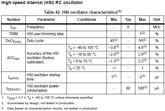
The HSI operates at 8MHz so that means ±23.2kHz. Over the course of an hour this could mean a drift of more than 10 seconds.
What about the external crystals? Well they’re much better with a typical tolerance of ±30ppm and can be found on most cheap MCU development boards.
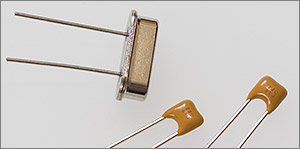
An 8MHz crystal running with a tolerance of ±30ppm would drift by a tenth of a second per hour or just two and a half seconds per day, temperature fluctuations not withstanding.
So that got me thinking. As long as I’m operating at a reasonably constant temperature then my data logger could apply a periodic correction to my timekeeping clock so that I’d have very accurate timings over a period of days.
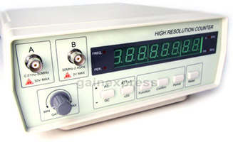
But how do I measure the accuracy of the crystal that’s clocking my MCU? The answer is with a frequency counter. Off to ebay I go. There’s a wide range of counters out there, from the cheapest bare-PCB options to the high-end laboratory grade equipment from the likes of HP (I hold out the hope that one day they’ll drop the comedy names and actually be HP again).
Opposite ends of the product spectrum
Occupying the middle ground there’s the no-name VC3165 unit that looked very tempting and can be had for about £60 from Hong Kong.
The VC3165 generic counter
I almost bought it but instead I somehow managed to persuade myself that it’d be a fun and educational project to design and build a frequency counter myself that could be used for general purpose measurement but would contain features tailored specifically to calibrating MCU clocks.
How frequency counters work
The executive summary is that a frequency counter works by counting the edges of the unknown frequency as well as the edges of an accurate reference over a fixed time period. Simple mathematics then tell you what the unknown frequency is, plus or minus an error term. There are a number of different methods for doing this, let’s take a look at them.
For the remainder of this article we will refer to the frequency being measured as the sample frequency and the accurate timebase as the reference frequency.
Direct frequency measurement
The direct frequency method counts the number of edges of the sample frequency observed during a fixed number of periods of the reference frequency.
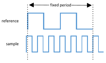
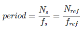
The formula for calculating the sample frequency is straightforward.

N is the count, period is in Hz
From the above formula you can see that if the reference frequency is 1Hz then the measurement implementation becomes really simple as the number of sample counts observed is the sample frequency and could be output directly to an attached display.
Because the time period is linked to the reference frequency the error term for this method is ±1 tick of the sample clock, making the error term variable for an instrument built to use this method of counting.
Equal precision measurement
The equal precision (or reciprocal) method links the time period to an integer multiple of the sample clock. There is an excellent and very readable PDF available online that describes this method. Click here to read it.
The instrument receives a trigger to start counting pulses but does not do so until the next rising edge of the sample clock. It then starts counting both the reference and sample clock edges using two counters.
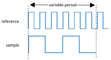
After the desired time period has come to an end the instrument stops counting at the next rising edge of the sample counter. The relationship between the time period, the two counters and their associated frequencies is given by the following ratios:
s and ref are the sample and reference signals
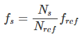
Discarding the period and re-arranging the remaining ratios gives us the following formula for calculating the sample frequency:
The advantage of this method is that the error term is ±1 tick of the reference clock and if the reference clock is high enough then the error term can be reduced to a very small value.
My frequency counter design
After studying the above counting methods I decided on the following goals for my frequency counter, which I’m going to call Nanocounter.
- Very accurate measurement over a range of 1 to 50MHz. This would cover the range of MCU crystals that I’d want to measure.
- Onboard accurate, but cost effective reference with the option to feed in an external reference clock source.
- Advanced options including data logging, charting and calibration of the onboard reference.
That should do for starters, let’s see how I get on. This project will call upon a large number of engineering disciplines including circuit design, PCB layout, SMD reflow, FPGA design, C++ programming and java android programming so I should be in for a fun time.
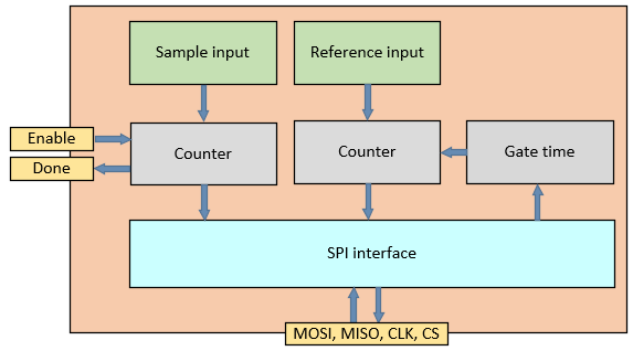
I’ve made the decision to use the equal precision counting method so let’s see how that looks in a block diagram of the whole system.
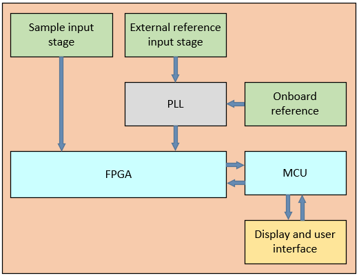
The input stage
My design should be able to accept a wide range of input signals including sine and square waves that are DC or AC coupled and range over the common voltages used to drive clock signals.
The job of accepting these signals and transforming them into a standard LVCMOS square wave that I can feed to the FPGA falls to the input stage or analog front end.
I’ll need to instantiate my input stage design twice, once for the sample clock input and again for the external reference clock input.

The PLL
The onboard reference clock will be a 10MHz oscillator and the external reference input, if connected, is expected to be of the same frequency. The PLL is used to multiply the 10MHz input up to the much higher reference frequency that is provided as an input to the FPGA. The actual reference frequency will be limited by the counting speed of the FPGA as well as the limits of the selected PLL.

The PLL used for this design will have to accept multiple inputs and have very good jitter characteristics if I am to maintain my goal of very high accuracy.
The FPGA
Here’s the business end of the system. An FPGA is capable of counting extremely quickly, in parallel, and on a cycle-accurate basis. While even the most basic MCUs have edge-triggered interrupts they cannot react quickly enough to count at the speed that an FPGA can achieve.
The MCU
The MCU marshalls all the other components in the system. It communicates with the user and the display, programs the FPGA on startup and holds system calibration data.
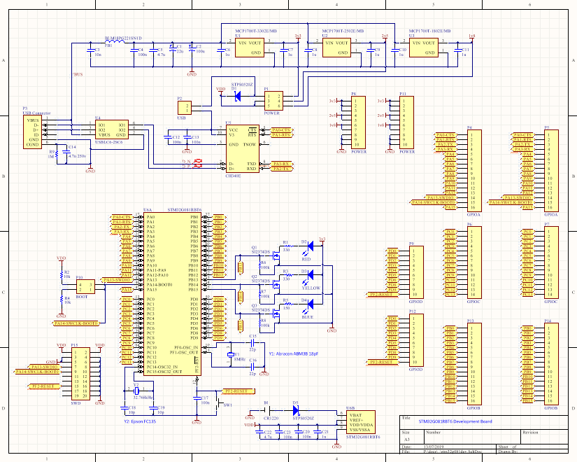
The circuit design
So, considering all that I’ve learned so far I came up with a circuit design for the complete system. This isn’t going to be a bargain-basement design. My requirement for high accuracy means that top quality components from the likes of Linear Technology and Analog Devices are going to be making an appearance on this board.
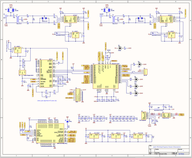
Click for PDF
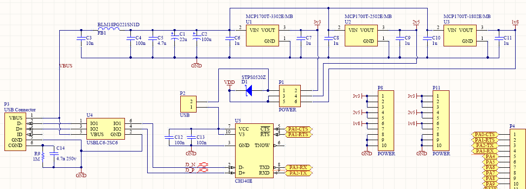
The USB port and power entry
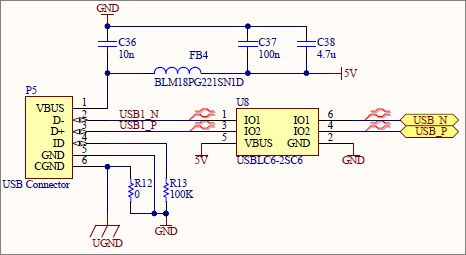
Power is supplied through a USB mini B socket. The potentially noisy 5V line is smoothed using capacitors and a ferrite bead. I know from my previous experience with FPGAs that they can be rather power hungry. If the power consumption goes above 500mA then I’ll need to restrict usage to USB 3 ports or charging plugs.
I’ve opted to hook up the D+ and D- data lines even though I may not use them in the final design. The USBLC6 ESD protection device from ST Micro provides protection against spikes on the line that may occur during the insertion and removal of the plug.
The sample and reference input stages
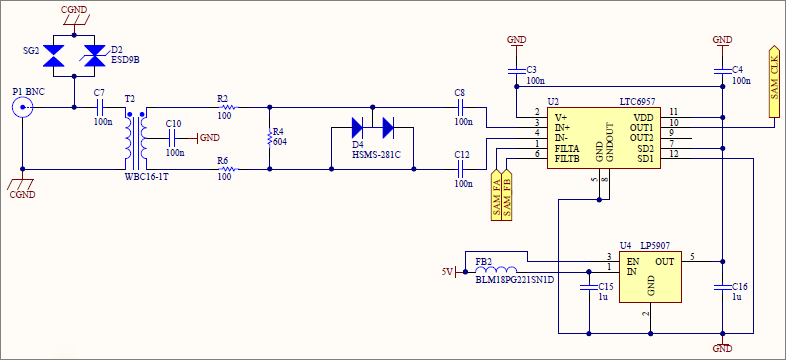
The input stage is based around the LTC6957 from Linear Technology. This device is a very low noise buffer and signal distribution device that can accept any sine or logic level less than 2Vp-p and output a fixed logical level.
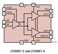
It’s available in 4 separate versions that can output LVPECL, LVDS or CMOS logic levels. I’ve selected the LTC6957IMS-3 variant that has CMOS output levels and costs about £5 plus tax from Digikey.
Linear Technology produce a very useful design note, DN514, that presents an example input circuit for the LTC6957 that does exactly what I need.
The spark gap, SG2 and ESD protection diode, D2, provide a level of defense against input voltage spikes that could occur during human interaction with the BNC connector. The capacitor C7 AC couples the input signal before it passes through the transformer, T2 and the schottky diodes provide voltage limiting to the inputs of the LTC6957. That’s a very brief summary of the operation. I’d encourage you to read DN514 for the full details as presented by Linear Tech’s engineers.
The LTC6957 comes with 3 selectable narrowband filter options of 500MHz, 160MHz and 50MHz. The best choice will depend on the input signal so I’ve opted to connect the filter pins to MCU GPIO pins so I can offer the choice of filter through the user interface.
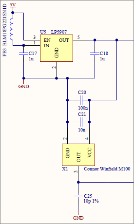
LP5907
I’m powering the LTC6957 from an LP5907 ultra-low noise LDO regulator from Texas Instruments.
The input stage in the illustration is the sample input. The external reference input is basically identical. The only difference is that I’ve connected the LTC6957 output shutdown pin to an MCU GPIO pin so that I can shutdown the output when the onboard reference is being used.
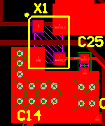
The onboard reference oscillator
The stability and tolerance of the reference clock is key to the accuracy of the frequency measurements. Clearly I need something more accurate than the crystals that I seek to measure which means in practice that I need to use either a temperature compensated oscillator (TCXO) or an ovenised oscillator (OCXO).
The price of these devices is in direct proportion to their stability and they get quite expensive really quickly. Since I’m providing the ability to supply an external reference when exceptional accuracy is required I’ve decided to go for a reasonably high end TCXO, the Connor Winfield M100F, which has a stability of ±100ppb and costs about £14 plus tax from Digikey.
More stable TCXOs exist, and then there are the very stable OCXOs but they’re beyond the scope of my requirements for this article. Cheap used OCXOs and VCOCXOs abound on ebay but I’d be very wary of them since the reason they’ve been decommissioned is that their age means that they could have drifted out of spec and for the VCOCXOs that means they could have drifted out of the range of voltage correction.
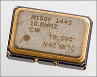
Connor Winfield M100F
The TCXO works by applying compensation to the output frequency based on a curve of temperature vs. offset that’s preprogrammed at the factory. A TCXO will still drift with change in temperature but it will do so at a much lower rate than a standard crystal (we’ll have some fun demonstrating this in the videos that accompany this article). Better immunity to ambient temperature changes can be had with an OCXO but they’re really expensive from the usual distributors —.
The datasheet for the M100 specifies an output load capacitance of 15pF. Deviation from this value could alter the output frequency by up to 20ppb per pF. I consulted the datasheet for my FPGA and found an input capacitance range of 3-10pF for input pins with no typical value specified. Hoping that it’ll be somewhere around 5pF I added C25 to the output to provide the additional load. It doesn’t matter too much if I’m off by a bit because the error is a constant and can be compensated for in calibration.
The PLL
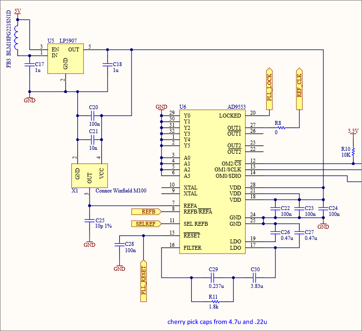
The purpose of the PLL is to multiply the reference frequency up to 200MHz for the FPGA to use to generate the high speed counter. Anyone familiar with the Xilinx FPGAs might be wondering at this point why I’m not using the built-in Digital Clock Manager (DCM) on the Spartan 3. The blocker for that idea is that the DCM minimum clock input is 18MHz and in any case the output RMS jitter is rather high at around 250ps compared to approximately 1ps for the device used here.
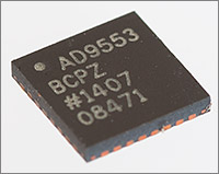
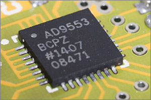
I’ve selected the Analog Devices AD9553 as the external PLL. It’s a very high quality, low jitter device available in an annoying QFN package.
The AD9553 is full of features and must be externally programmed over SPI before it’ll lock on and generate my target frequency frequency.
The Ax and Yx pins can be used by the AD9553 to hard-select from a range of predefined configurations and can be used as an alternative to SPI programming. Grounding all these pins selects SPI as the active configuration mode and gains access to far more options.
The AD9553 supports two separate inputs and has a pin to select between those. I use these to connect the onboard TCXO and the external reference input and use GPIO from the MCU to select between them.
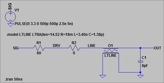
The 200MHz LVCMOS output is presented on pin 27. I placed a footprint on the board for a series termination resistor in case I need to suppress any ringing on the output. The best way to check if you’re going to have signal integrity issues on a high frequency line is to simulate it as a transmission line using the LTSPICE circuit simulator.
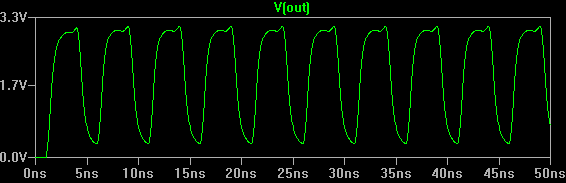
I ran a simulation and the projected output signal looked fine to me so R8 is specified to be 0Ω.
C29, C30 and R11 form the external part of the PLL loop filter. There’s a guide to selecting suitable values for these components in the AD9553 datasheet but far better to use the free AD9553 evaluation software from Analog Devices. It’s one of those quirky programs that has limitations and sometimes crashes but contains such critical functionality that you’ll forgive all for the information it provides.
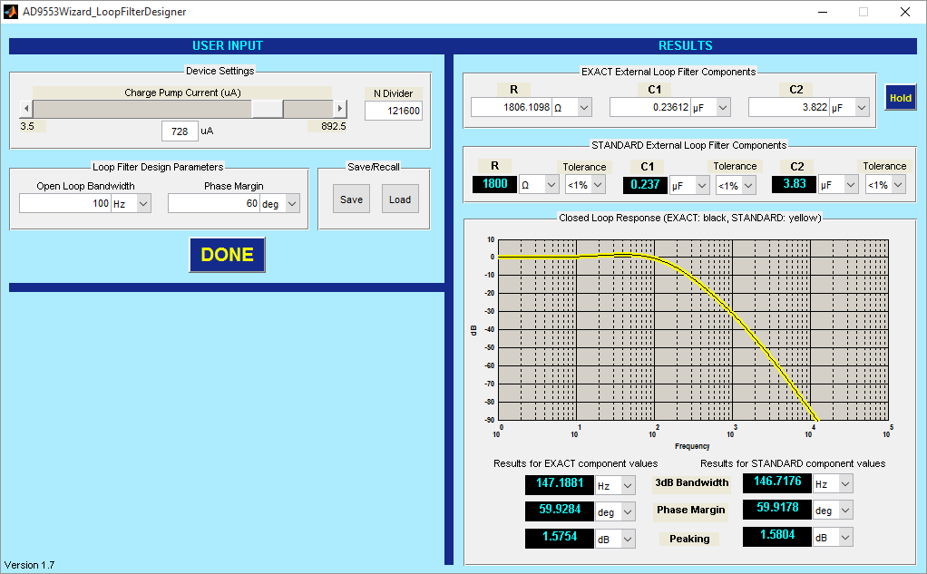
The challenge with the loop filter designer is to get it to generate standard values for the capacitors and resistor. In the end, after spending ages in this tool, I selected the above values. I’d already bought some 1% 1800Ω resistors so it wasn’t hard to find one that measured almost exactly nominal. The caps were harder. I’d selected the loop filter values so that they fell within the 20% tolerance of some X5R ceramics that I already had in stock and so I spent some time measuring caps until I cherry-picked two that fell very close to what I needed. I probably went through 20 each of my 0.22µF and 4.7µF caps before finding some that were within 1% of the loop filter values.
When I’d finished with the loop filter designer the tool was able to generate a very useful interactive block diagram.
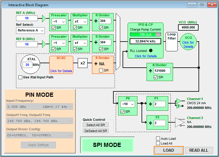
The interactive diagram is preloaded with the settings from the loop filter designer so you just have to make any tweaks to the input and output configurations and then it will generate the SPI register settings for you.
I can’t overstate how useful this tool is and Analog Devices deserves a huge thank you for providing it and saving us hours of error-prone poring over datasheets and application notes. I know who’ll be getting my custom in the future.
The FPGA
I selected a Xilinx Spartan 3 XC3S50-5 FPGA to do the grunt work of the high speed design.
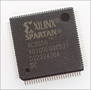
This is an older model than the current Spartan 6 generation but I know it well having used it in my FPGA Graphics Accelerator project and besides I have more than 400 of them to find a use for. No that’s not a typo, I actually picked up 450 of these as new and sealed surplus stock on ebay for a bargain some time ago. Look, here they are!
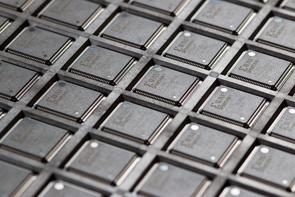
A sea of programmable logic
I/O capacity is no problem in this design. I only need the two clock inputs and some control lines from the MCU. FPGA_CS, FPGA_SCLK, FPGA_MOSI and FPGA_MISO are an SPI interface for talking to the MCU.
The FPGA_CEN is an count enable input pin that will cause counting to start on a rising edge. FPGA_CDONE is an output pin that will transition to high when the gate time is completed.
The model is that the MCU will use the SPI interface to load a gate counter value and then set FPGA_CEN high. When the gate counter is reached FPGA_CDONE will go from low to high and then the MCU will use the SPI interface to read out the two counter values. The FPGA is then idle until the next rising edge of FPGA_CEN.
I follow Xilinx’s guidelines for decoupling which results in rather a lot of capacitors that need to be placed around the device.
This is probably overkill for this design but caps are cheap and the last thing I want to be doing with my prototype is debugging an unstable design due to insufficient decoupling.
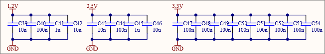
Running the rest of the board at 3.3V means that I need three power supplies for the FPGA.
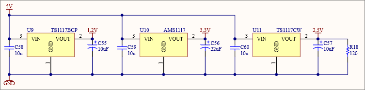
The 1.2V supply is used for the FPGAs internal logic, the 2.5V supply is an auxiliary source of power used primarily to optimize the performance of various FPGA functions such as I/O switching and the 3.3V supply is used to power the output drivers.
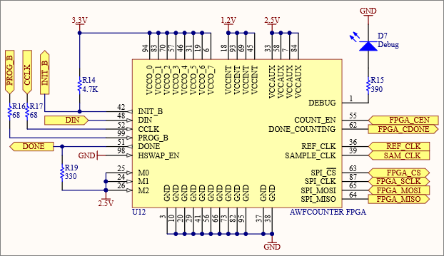
This model of FPGA does not persist your design while the power’s off. When you apply power you need to do a bit of a dance with a selection of programming pins to load the design bitstream into the core before it will run. The INIT_B, DIN, CCLK, PROG_B and DONE pins on the left of the schematic image are used for programming and are controlled by the MCU.
The programming mode, called Slave Serial by Xilinx is co-ordinated by the MCU. I store the FPGA design in the MCU flash and load it into the FPGA from there as the first task after reset. There’s a bit of a hurdle to be overcome in that some of the FPGA programming pins are referenced to the 2.5V supply and are not 3.3V tolerant. Thankfully Xilinx recognised this limitation and publish XAPP453, a guide to programming the Spartan 3 using a 3.3V controller.
Debugging an FPGA design in-circuit is difficult in the extreme which is why I simulate every aspect of it before going anywhere near a circuit design tool. I’ve included a DEBUG pin attached to an LED that I can use as an indicator to help with any last-ditch debugging.
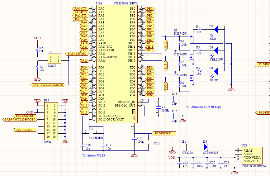
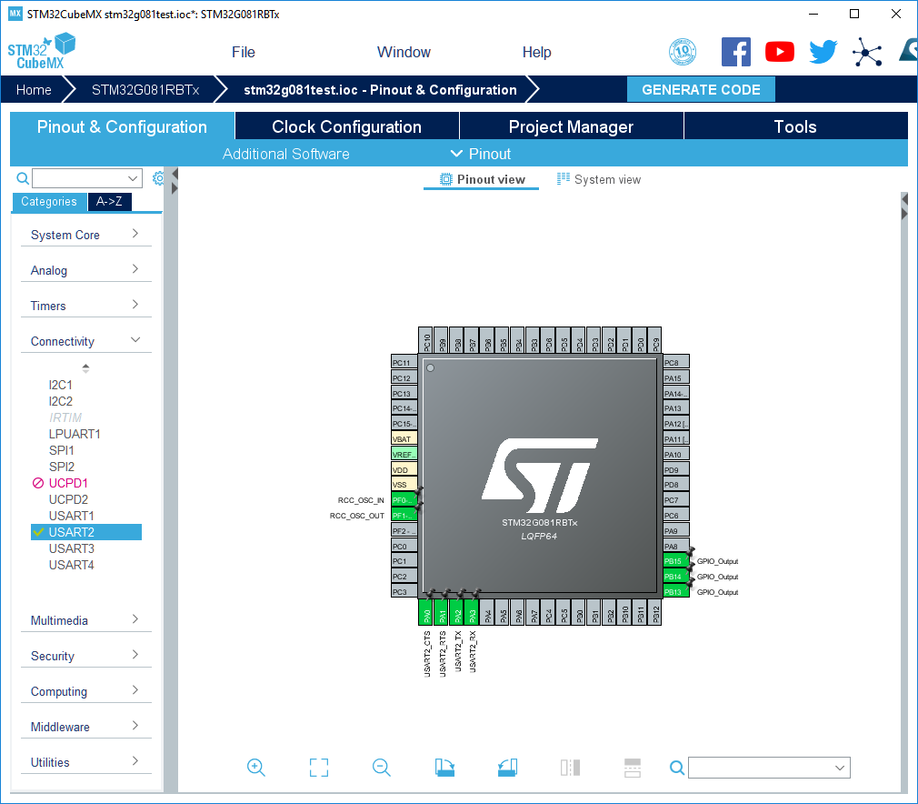
The MCU
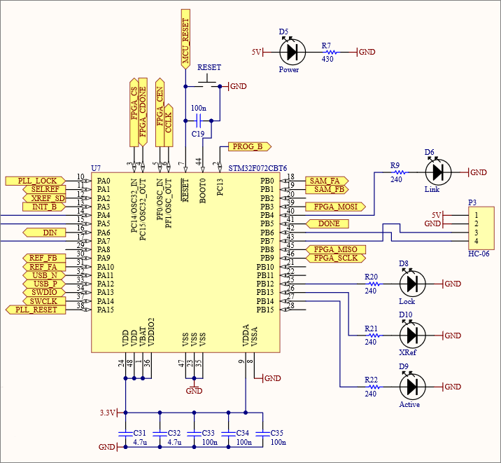
The MCU that I’ve selected for this design is the STM32F072CBT6 in a 48-pin LQFP package. The 48-pin package gives me just enough I/O to complete this design and this 072 model comes with 128kb flash and 16kb SRAM. The large flash space was the key reason for the selection of this model because I’ll be compiling in the FPGA bitstream which will require around 60kb.
A nice extra is the inclusion of a USB PHY in this device. I’ll connect up the USB data lines just in case I decided to do something with them in future. In common with all F0 models, this one runs a core clock of 48MHz and can source that clock from an internal PLL fed by a built-in internal 8MHz oscillator.
Most of the I/O is self explanatory. You’ll see the FPGA, PLL and LTC6957 control pins as well as the USB data lines and the SWD programming pins. I’m including a full 20 pin header that will connect directly to the ST-Link/v2 programming device.
A number of status LEDs are provided. The power LED is self-explanatory. The link LED will provide an indication of recent bluetooth activity. The lock LED will light when the PLL is locked. The xref LED will light when the external reference is selected as the active input and the active LED will light when the FPGA is actively counting.
Bluetooth connectivity is provided by the cheap and easy to use HC-06 module that I’ve used before in my Android Reflow Oven project.
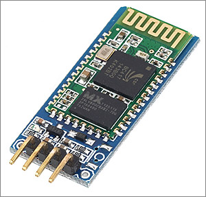
The HC-06 bluetooth board
The HC-06 pairs to an Android device without MCU intervention and, once a connection is established you can just treat it as a 9600/8/N/1 UART.
Bill of materials
Here’s a complete bill of materials for this design. The capacitors should be X5R or X7R. Where tolerance is important I’ve noted it in the description.
| Identifiers | Value | Quantity | Footprint | Description |
|---|---|---|---|---|
| C1, C2, C3, C4, C5, C6, C7, C8, C9, C10, C11, C12, C19, C20, C22, C23, C24, C28, C33, C34, C35, C37, C40, C44, C47, C48, C49, C50, C51, C52, C53, C54 | 100n | 32 | 0603 | Ceramic capacitor |
| C13, C14, C15, C16, C17, C18, C41, C45 | 1µ | 8 | 0603 | Ceramic capacitor |
| C21, C36, C39, C43 | 10n | 4 | 0603 | Ceramic capacitor |
| C25 | 10p 1% | 1 | 0603 | Ceramic capacitor |
| C26, C27 | 0.47µ | 2 | 0603 | Ceramic capacitor |
| C29 | 0.237µ | 1 | 0603 | Ceramic capacitor |
| C30 | 3.83µ | 1 | 0603 | Ceramic capacitor |
| C31, C32, C38 | 4.7µ | 3 | 0603 | Ceramic capacitor |
| C42, C46, C58, C59, C60 | 10µ | 5 | 0805 | Ceramic capacitor |
| C55, C57 | 10µ | 2 | 1206 | Tantalum capacitor |
| C56 | 22µ | 1 | 1206 | Tantalum capacitor |
| D1, D2 | 2 | SOD-923 | ESD supression diodes (optional) | |
| D3, D4 | HSMS-281C | 2 | SOT323-3AN | dual Schottky diodes |
| D5, D6, D8, D9, D10 | LED | 5 | 3mm through hole | 3mm LEDs, various colours |
| D7 | 1 | 1206 | Surface mount LED | |
| FB1, FB2, FB3, FB4 | BLM18PG221SN1D | 4 | 0603 | Ferrite bead |
| P1, P2 | 2 | BNC PCB Connector | BNC connector | |
| P3 | 1 | 2.54mm | 4x1 HC-06 header | |
| P4 | 1 | 2.54mm | 10x2 SWD header | |
| SG1, SG2 | Spark gap | 2 | Custom | PCB spark gap |
| R1, R2, R5, R6 | 100 | 4 | 0805 | SMD resistor |
| R3, R4 | 604 | 2 | 0805 | SMD resistor |
| R7 | 430 | 1 | 0805 | SMD resistor |
| R8, R12 | 0 | 2 | 0603 | SMD resistor |
| R9, R20, R21, R22 | 240 | 4 | 0805 | SMD resistor |
| R10 | 10k | 1 | 0805 | SMD resistor |
| R11 | 1.8k | 1 | 0805 | SMD resistor |
| R13 | 100k | 1 | 0603 | SMD resistor |
| R14 | 4.7k | 1 | 0603 | SMD resistor |
| R15 | 390 | 1 | 0805 | SMD resistor |
| R16, R17 | 68 | 2 | 0805 | SMD resistor |
| R18 | 120 | 1 | 0603 | SMD resistor |
| R19 | 330 | 1 | 0603 | SMD resistor |
| RESET | 1 | Custom | Pushbutton | |
| T1, T2 | WBC16-1T | 2 | Custom | Coilcraft transformer |
| U1, U2 | LTC6957 | 2 | MSOP12 | Dual Output Buffer/Driver/ Logic Converter |
| U3, U4, U5 | LP5907 | 3 | SOT23-5AM | 3.3V low noise regulator |
| U6 | AD9553 | 1 | QFN32 5x5 | PLL |
| U10 | AMS1117 | 1 | SOT223-4N | 3.3V regulator |
| X1 | Connor Winfield M100 | 1 | Custom | 10MHz TCXO |
| P5 | USB connector | 1 | Custom | USB Mini B surface mount |
| U7 | STM32F072CBT6 | 1 | LQFP-48 | STM32 F072 MCU |
| U8 | USBLC6 | 1 | SOT23-6 | USB ESD protection |
| U9 | TS1117BCP | 1 | TO-252 | 1.2V regulator |
| U11 | TS1117CW | 1 | SOT223-4N | 2.5V regulator |
| U12 | XC3S50 | 1 | VQ100 | Xilinx XC3S50 Spartan 3 FPGA |
| HC06 | Bluetooth board | 1 | 4x1 2.54mm | HC-06 Bluetooth board |
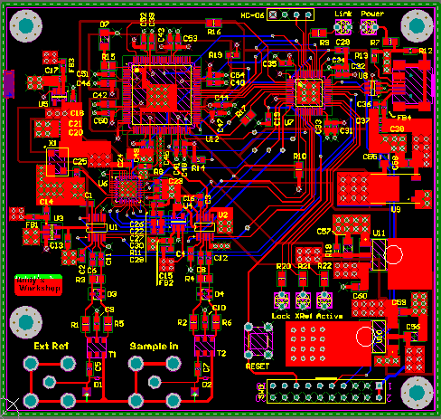
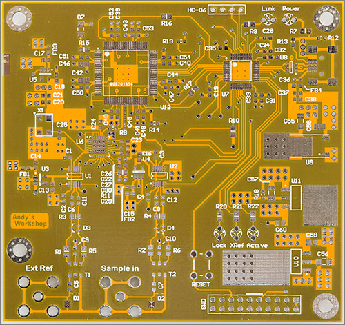
Board layout
Now I’ve got a schematic that I’m happy with it’s time to consider the board layout. I’ve already decided that this is going to be a four layer board with a stackup that looks like this.
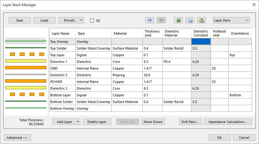
The main driver for choosing four layers instead of the cheaper two layers is that I’ve got both analog and high speed digital circuits on this board and I really want a continuous unbroken ground plane beneath the top signal layer to help with signal integrity and allow me to have controlled impedance traces. I’ll also benefit from simpler routing around the FPGA with the ability to run all those different power supplies through an inner plane.
Click for a larger image
I want to use the great value prototyping services from PCBWay, ITead, Seeed and others which means that I really need to keep the board size to 10x10cm because there’s a large price jump for four layer boards above that level.
Most of the signals, including all the 50Ω controlled impedance traces are on the top layer with the bottom layer used for additional routing. Large copper fills with multiple vias to the solid ground plane are located near to each of the sensitive components so that they have a low noise, low impedance path to ground.
Local fill with multiple vias to ground
The digital components, primarily the FPGA and the MCU are located such that their return signals through the ground plane do not pass under the analog components. Furthermore, chassis ground for the BNC connectors is isolated from the PCB ground.
My previous FPGA design, the graphics accelerator, drew more current from the 3.3V supply than I was expecting, resulting in the AMS1117 regulator getting rather hot. I’ve learned my lesson from that and have included large exposed copper fills around the FPGA regulators that can be used to dissipate the heat throughout the PCB.
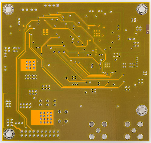
Large heatsink area for the AMS1117 is also mirrored on the bottom layer
The fill next to the AMS1117 is sized to accept one of those little RAM IC heatsinks that you can get on ebay. I don’t know if I’ll need one at this stage but there’s room for overkill on this board so better to be safe than sorry.

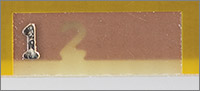
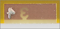
Layer stack telltale
Over on the left of the board you can see a row of numbers. This is a trick I use to make sure that the manufacturer gets the layer stackup correct. I include the numbers 1..4 sequentially in the copper on each layer from top to bottom and remove the solder mask from top and bottom and the copper from around the numbers so that I can see through the board when it’s held up to the light. If the manufacturer has got the inner layers the right way around then I’ll be able to view the 1..4 sequence with decreasing brightness from front to back.
I made a small mistake in my implementation of this feature in that I forgot to remove the copper from the inner layers surrounding the numbers. The feature still works though. If the manufacturing is correct then I will be able to see 1,2 when viewed from the top and 3,4 when viewed from the bottom.
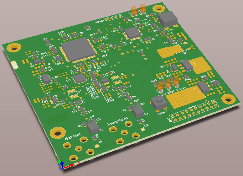
The 3D view of a board is not just for show, it’s really useful for checking to see if you’ve made common mistakes such as overlapping component labels or labels straying over vias or pads.
Manufacturing the board
Elecrow is my normal go-to provider for two layer manufacturing because their prices are so good. Four layer is more pricey though and anything above 5x5cm sees a large rise in the manufacturing cost. This board is a 10x10cm layout and at the time of writing PCBWay was the best price available.
I’d never used PCBWay before and a quick google around revealed that the online reviews cannot be trusted because PCBWay will pay reviewers for positive reviews posted on internet forums and websites. I really wish they’d stop this because if the service is good then the reviews will come naturally. I’m going to relay my honest experience here with the hope that you can trust me not to make stuff up just to get a few dollars off my next order.
Anyway, I picked the yellow soldermask because this PCB will be exposed and I’d like it to look more distinctive than the standard green. Because I’m going to be doing controlled impedance traces I needed to know the PCB dielectric constant and the thickness of the PCB copper and FR4 substrates. My emails to PCBWay were answered within 24 hours by Lynne and I got the answers I needed. The dielectric constant is 4.29 and the upper and lower layers are 18µm copper (note that since this was written they’ve now changed to 35µm).
I selected the China post option which means the standard 2-4 weeks went by before the boards arrived.
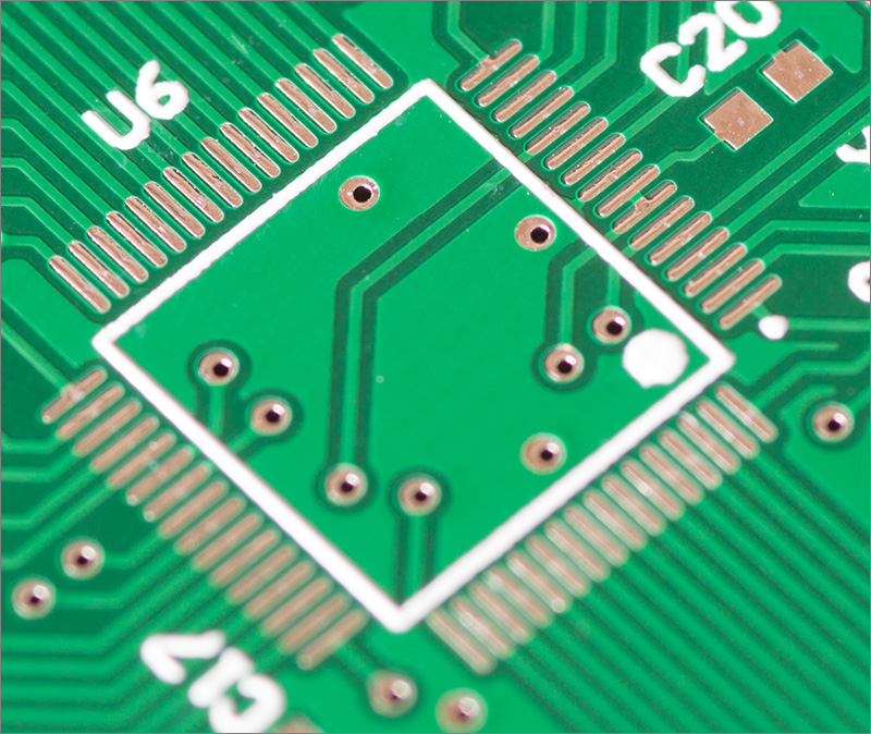
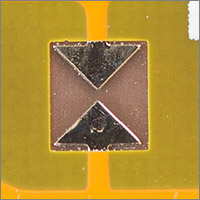
The boards look great to me. What’s really important is that they’ve managed to get complete and unbroken soldermask slivers between the tiny pads of the QFN.
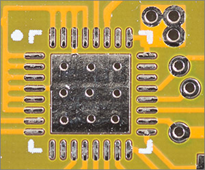
The QFN is by far the most annoying and difficult part to reflow and frankly you need all the help you can get. Having soldermask there to prevent bridges will play a big part in my chances of a successful reflow.
If you look at the upper and lower right corners of the QFN you’ll see that I’ve used side-exit traces from the pads. Be careful when you do this because QFNs with a ground pad have that pad held in place by very small metal spurs that are exposed from the package at the end of the row of pins. If you don’t have solder mask covering your traces then there’s a small but real risk that you could accidentally ground a trace.
The drill positioning for the vias also looks great for a prototype service and the soldermask apertures appear to be well positioned with good tolerance. The silkscreen has the familiar dot-matrix low resolution style that you get with prototype services.
I’ve heard that the prototype services use different board houses for four layer manufacturing and that may account for the better quality results and higher price to go with it.
Here’s a shot of the back and front layer stack tell tales. I can see that they’ve got the stack correctly ordered so my controlled impedance traces will be correctly referenced to the ground plane.
Here’s my attempt at a spark gap. That’s an 8 mil gap between the two pointy ends. Do they work? I don’t know for sure but they’re free so I may as well include them. If you’ve never seen one before and don’t know what they do then there’s an entertaining video over at the eevblog that’ll tell you all that you need to know and plenty that you didn’t expect!
Building the board
To build the board I followed my usual process of tinning the pads, applying flux and then balancing the components on the tinned pads. The board is then carefully placed in my reflow oven and I execute a ‘leaded’ reflow profile. At around 180°C the little bumps of solder melt and the components sit down onto the pads.
The QFN is of course the biggest unknown in the process because of the ground pad that’s completely hidden from view. The ground pad must be connected and it must also have multiple via connections to a solid plane. The trick is getting just enough solder so that it will sit down onto the board at the same level as the surrounding pads and the solder must not wick away down the vias leaving you with nothing left on top. Of course you can’t visually check that you’ve got it right after the reflow, nor can you touch it up if you get it wrong.
If the pad is the device’s only connection to ground then you can test its continuity by probing the little supporting spurs that are exposed at the end of the rows of pads. I really dislike the QFN package but they’re here to stay so developing a repeatable assembly process is really important.
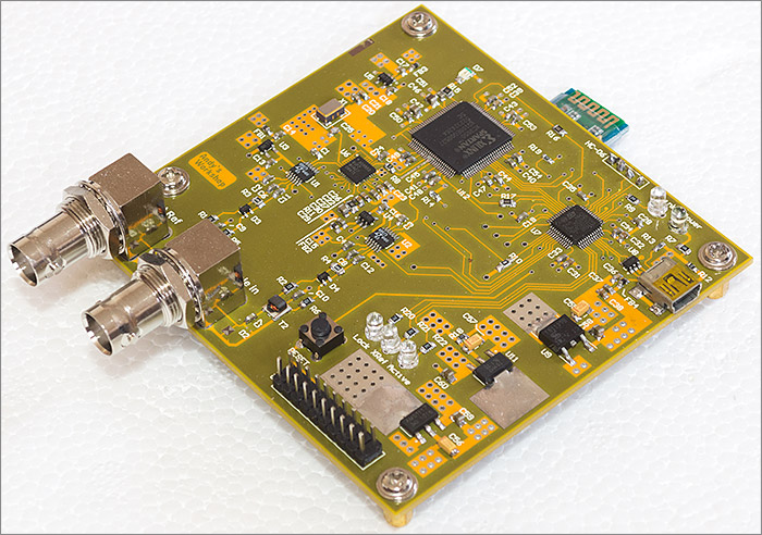
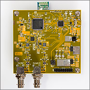
Here it is fully assembled and looking great in my opinion. I’ve opted to stick the HC-06 underneath the board with a double-sided sticky pad and connect it with wires to the 2.54mm header on the main board. It’s designed to stick out by about 20mm so that the bluetooth antenna is not obstructed.
The FPGA design
A block diagram of the FPGA design is shown above. It’s quite simple but does require some high speed processes. The flow of control works like this.
- The MCU programs a gate counter using the SPI interface.
- The FPGA receives a rising edge on its ‘enable’ input.
- Counting begins at the next rising edge of the sample input and ‘done’ goes low.
- When the reference counter reaches the gate limit counter then counting stops at the next rising edge of the sample clock.
- Done goes high.
- The MCU reads the two counters using the SPI interface.
It’s all quite straightforward and you can view the VHDL source code here on github. The important parts of the system are the 31-bit counters, and in particular the reference counter. These must be able to cope with counting at 200MHz. The choice of counter width is a trade off between counter speed and the maximum counter value. At 31 bits I can cope with up to 10 seconds of counting and hence the maximum gate time is 10 seconds.
A typical synchronous counter, of the type automatically created for you by the synthesiser when you use an addition-by-one expression, is not fast enough to count at 200MHz. To get to that sort of speed requires a faster implementation and I chose to reuse one available here at opencores.org.
The side effect of using a pipelined counter such as this is that counting takes more than one clock cycle. In this design that means that several clock cycles are used after the gate time has ended to flush the pipeline and let the counter settle. This can be seen in this ISIM simulation screenshot. Notice how the counters continue to update for a few clock cycles after the done_counting bit is set.
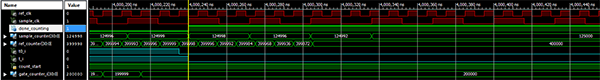
Pipelined counter operation (click for larger)
Xilinx ISIM… oh dear the bitrot really is starting to affect these venerable old tools. On Windows 7 ISIM was stable but clunky to use but now on Windows 10 it’s started to crash during certain common UI operations. Xilinx aren’t interested so it looks like the only solution if you need crash-free operation is to run Windows 7 in a VM.
To ensure that my timing goals are met I add timing constraints to the .ucf file:
TIMESPEC TS_ref_clk = PERIOD "ref_clk" 5 ns HIGH 50 %;

NET "inst_equal_precision_counter/ref_clk_div" TNM_NET = "inst_equal_precision_counter/ref_clk_div";
TIMESPEC TS_ref_clk_div = PERIOD "inst_equal_precision_counter/ref_clk_div" 10 ns HIGH 50 %;

NET "sample_clk" TNM_NET = "sample_clk";
TIMESPEC TS_sample_clk = PERIOD "sample_clk" 20 ns HIGH 50 %;

NET "spi_clk" TNM_NET = "spi_clk";
TIMESPEC TS_spi_clk = PERIOD "spi_clk" 20 ns HIGH 50 %;
Inspecting the verbose output from the post-PAR timing report shows whether I’ve managed to meet my timing constraints:
Timing constraint: TS_ref_clk = PERIOD TIMEGRP "ref_clk" 5 ns HIGH 50%;
For more information, see Period Analysis in the Timing Closure User Guide (UG612).

 120 paths analyzed, 120 endpoints analyzed, 0 failing endpoints
 0 timing errors detected. (0 setup errors, 0 hold errors, 0 component switching limit errors)
 Minimum period is   2.592ns.
All my constraints are met and this design can run well in excess of the 200MHz target. There’s no point in optimising any further once all constraints are met so it’s time to move on to the next part of the design.
The MCU and android programs
The MCU exists to program the FPGA and PLL and then continually service requests arriving over bluetooth from the app. Let’s take a look at the app design. Here’s the main display screen.
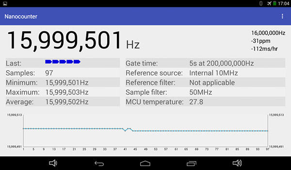
The display area is dominated by the measured frequency display at the top. The number of decimal places can be customised (none shown here) and I can opt to display the value in Hz, kHz or MHz.
The table in the center of the screen shows a number of statistics that are continually updated as samples are gathered.
The chart at the bottom shows how the measured frequency has changed over time and can be used to get a quick visual idea of the stability of the measured source.
The three numbers at the top right allow me to compare the measured frequency with the nominal value for this source and show the offset in ppm as well as the number of milliseconds per hour that a counter based on this frequency must be adjusted by in order to maintain accurate time.
Many settings can be customised, so let’s see the settings menu that’s accessible from the drop-down menu button at the top-right of the screen.
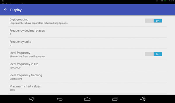
The first of the two available settings screens allows me to change aspects of the display. Changes to these settings are persisted locally on the android device. I can control how the frequency is formatted for display, what the ideal (nominal) frequency is and how many values the chart at the bottom of the screen should remember before resetting.
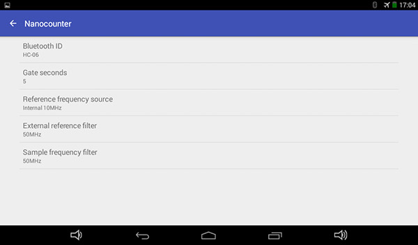
The settings on this screen control how the app interacts with the nanocounter device. I can change the bluetooth device ID, the number of seconds of measurement time (the gate time) as well as the reference frequency source and the filters applied by the two LTC6957 devices.
Changes to these settings are persisted locally on the android device as well as transmitted to the MCU when they are changed and when the app starts up so that the MCU can apply them accordingly.
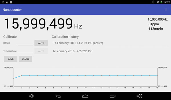
Calibration of the on-board reference clock is important because a TCXO has a temperature variance, albeit a much smaller one than a standard crystal, and will drift over time as it ages. The app allows me to capture a temperature offset and the current ambient temperature.
Calibration settings are written to a flash page on the MCU and a history of up to 112 settings can be stored. When the app starts up it reads the calibration array from the MCU and applies the most recent one to the session. Calibration settings are not applied when the external reference clock is selected.
The source code for the android app is available on github. Feel free to take a look around. The app is also available on the Google Play Store. Searching for ‘Nanocounter’ should find it.
The MCU program
The MCU program uses my stm32plus library to communicate with the peripherals. There’s no direct support in the library yet for the 072 series but I’m only using peripherals that are also present on the 051 which is supported so I build against the 051 and use adjusted startup and linker scripts to cater for the larger memory sizes in the 072.
The program is mostly asynchronous but there is a main loop in Program.h that performs some work.
  for(;;) {

    // check the command processor for activity

    _commandProcessor.run();

    // if the lock is lost then stop

    if(!_pllLockState && _frequencyCounter.isStarted())
      _frequencyCounter.stop();

    // if not started, locked and counters have been processed then start

    if(_pllLockState && !_frequencyCounter.isStarted() && !_countersReady)
      _frequencyCounter.start();

    // new counters available?

    if(_countersReady) {

      MillisecondTimer::delay(10);

      // read from the FPGA

      _frequencyCounter.readCounters(counters);

      // stop (reset) the counters inside the FPGA

      _frequencyCounter.stop();

      // set the latest counters inside the command processor

      _commandProcessor.setCounters(counters);

      // reset for a new run

      _countersReady=false;
    }
  }
The command processor run() method simply keeps the ‘link’ LED lit if there has been any bluetooth activity in the last second. Bluetooth commands are received and processed completely asynchronously.
A USART DMA channel is used to receive the command from the app and then I get an interrupt to tell me it’s ready. I then process the command in the IRQ context and initiate a USART DMA tranmission to send the response back to the app.
The device cannot function unless the PLL is locked so there’s an emergency stop feature if the lock is lost. The ‘lock’ LED is also lit up as long as the PLL is locked. I don’t need to poll for this because I’m using the STM32 EXTI feature to get an interrupt when the state of the PLL lock GPIO pin changes.
The rest of the loop just goes around in a loop starting a counting session on the FPGA, checking if it’s done (another EXTI interrupt) and if so then reading the final counters back and making them available to the app.
All the source code is of course free and available here on github.
Testing
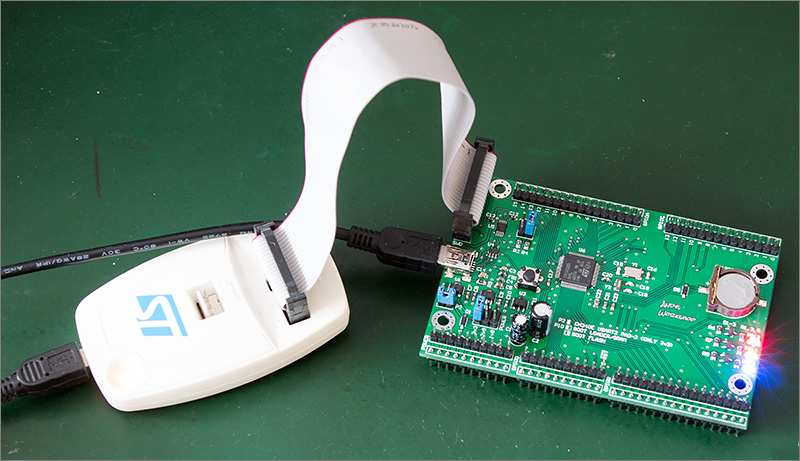
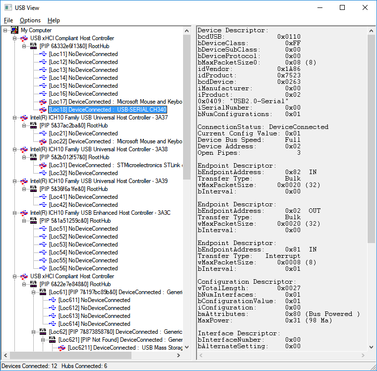
Oh this was a tale of ups and downs. After assembly the first thing that I did was attach the ST-Link/v2 programmer and check if the MCU was alive. It was. Check that one off the list.
I then set about writing the code that loads the FPGA bitstream into the FPGA. Success again. I’m on a roll here.
Next I need to program the PLL so I wrote the SPI code to load the register values to it. The registers loaded OK but oh no the PLL doesn’t lock. Not good. Not good at all. The AD9553 has some basic debugging features built in to it that allow you to route some of the internal clocks to the ‘lock’ pin and that can help you determine where the fault lies.
The only clock that gave me anything at all was the PFD reference input. At least that showed that the input clock multipliers and dividers were working. The device wasn’t totally broken. I put the board under the microscope and inspected the pads along the side of the QFN. Everything looked good. Suspicion naturally fell on the ground pad because I can’t see it to check it. All I could tell was that the solder bump on the ground pad had definitely melted because the QFN had sat down flush to the board. But what if the solder had wicked down the vias? It didn’t look like it from below. I spent hours fiddling with the debug settings in the AD9553 and was just about ready to give up when I posted a question detailing the symptoms in the ADI forums.
Something wasn’t right in there
Programming the AD9553 involves writing the registers, commiting them to the device and then calibrating it, after which you should get a lock. An engineer replied that the order of the calibration commands that I was issuing didn’t look right and suggested a fix. It worked! I got a PLL lock and have never failed to get a lock ever since. I can’t thank the ADI engineers enough that they take the time to answer hobbyist questions on their forums.
Now it’s time to fire up the Android app and check out the entire thing, front to back. There’s actually a gap of a couple of months here as I wrote the app over the course of some free evenings and weekends.
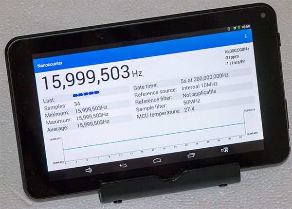
The app running on my cheapo £35 7″ tablet
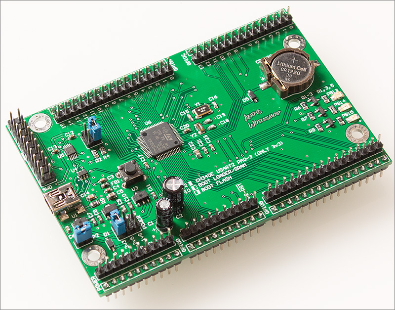
Here we can see the app measuring the performance of a 16MHz crystal on board a no-name Arduino Uno board that I got on ebay for a couple of pounds. This sort of board is going to be using the absolute cheapest components that they can source so I wasn’t expecting great performance from the crystal. I was actually quite surprised to find that it’s running at only 31ppm off the nominal frequency. You can see from the panel at the top right of the display that I would need to correct a clock based on a millisecond counter within the MCU by subtracing 111ms from the count each hour.
Calibration
Calibrating the device requires me to use an external frequency standard to measure the actual performance of the onboard TCXO. The easiest way to do this is to connect up the frequency standard to the sample input port.
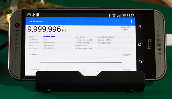
Measuring the onboard TCXO with the app running on my phone
The frequency standard that I’m using is a GPSDO with a 10MHz output. GPSDOs are very interesting devices and I’ll be publishing reviews and videos on the one that I’ve got in a future article.
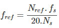
Because the frequency standard is known to be as near-as-who-cares to 10MHz the value that you see on the display is the performance of the onboard oscillator. If we rearrange the sample frequency equation given at the start of this article so that it yields the reference frequency before the x20 factor of the PLL we have:
Comparing the two equations shows that the frequency of the onboard TCXO is 10MHz+(10MHz-displayed value). In other words, it’s 10,000,004Hz at my current room temperature of 21.6°C.
To see how that value of 379ppb compares to the specifications produced by Connor Winfield we need to refer to the datasheet.
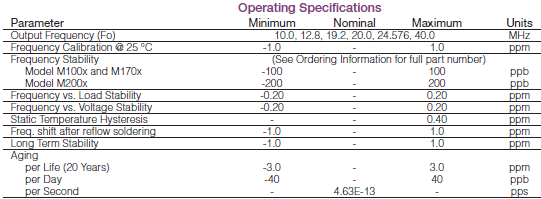
Unfortunately I can’t do an accurate calculation because all the reference figures are given at 25°C but I can see that my figure of 379ppb is well within the ±1ppm factory calibration range.
Watch the video
I’ve cobbled together a video in which you can see me using Nanocounter in various different scenarios. I’ll measure the frequency of a couple of crystals and then hook up my GPSDO frequency standard for comparison.
Get the design files
If you’d like to modify the design files, or just want to upload the Gerbers to a PCB printing service then you can download them in a zip file from my downloads page. Click on the Hardware schematics and CAM files tab at the top of the page.
Final words
I hope that you’ve enjoyed reading this project as much as I’ve enjoyed building it. If you’ve got anything to say then please feel free to leave comments down below or use the forum to start a longer conversation.